The Ultimate Guide to RF Sputtering
As an advanced thin film deposition method, RF sputtering has been widely used in modern industrial production and scientific research due to its unique advantages. From the preparation of semiconductor films in electronic devices to the functional coating of optical components.
- High Film Quality
- Strong Parameter Controllability
- Wide Range of Applicable Materials
- Realizing Multi-layer Composite Films
- Achieve Uniform Deposition Over Large Areas
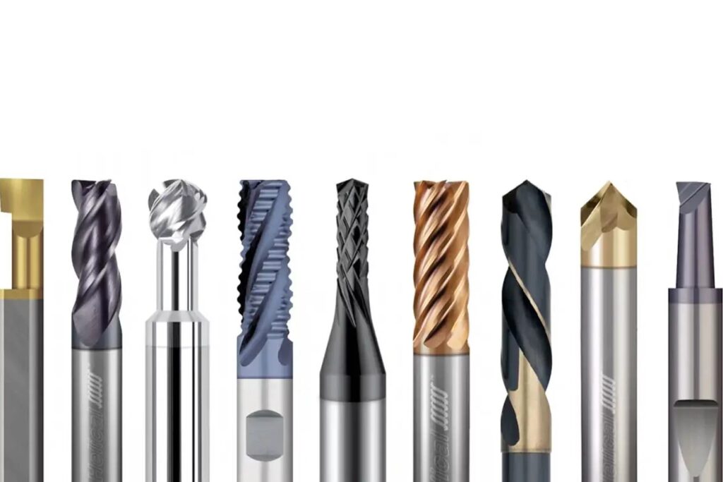
Wstitanium Workshop
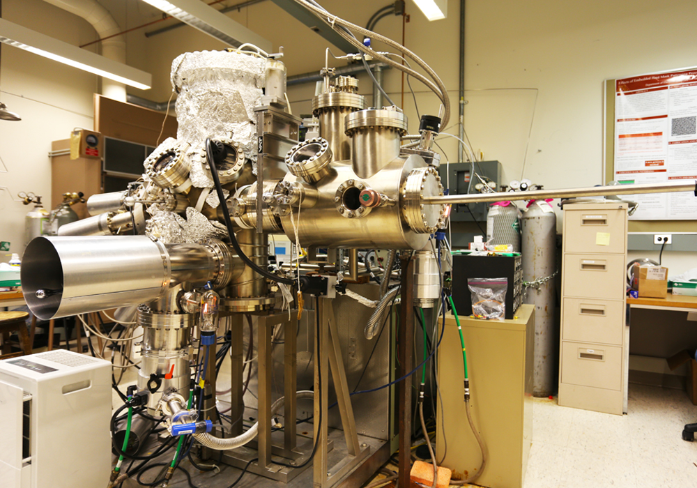
Our Powerful Facilities
Everything You Should Know About RF Sputtering
RF sputtering technology has gone through nearly a hundred years of development and innovation from early scientific exploration to today’s industrial application. It not only solves the sputtering problem of insulating materials, but also promotes the application of thin films in multiple disciplines with its unique advantages. As materials science continues to develop towards functionalization, integration, and miniaturization, RF sputtering technology continues to innovate, providing indispensable technical support for the discovery of new materials and the upgrading of devices.
RF sputtering is a technology that uses an alternating electric field generated by a radio frequency (RF) power supply to achieve thin film deposition. In an RF sputtering system, the RF power supply is usually connected to the sputtering target, and an inert gas (such as argon) is introduced into the sputtering chamber under a vacuum environment. The high-frequency electric field generated by the RF power supply ionizes the inert gas to form a plasma. The positive ions in the plasma are accelerated under the action of the electric field to bombard the surface of the target material, sputtering the target atoms. These sputtered atoms are deposited on the surface of the substrate and gradually form a thin film.

RF sputtering uses an alternating electric field. In each cycle, when the target is in the positive half cycle, electrons flow to the target surface to neutralize positive charges and accumulate electrons, making the target surface negatively biased; in the negative half cycle, the negative bias attracts positive ions to bombard the target, thereby achieving continuous sputtering of insulating target materials. This unique working principle allows RF sputtering to be used to deposit thin films of almost any solid material, including conductors, semiconductors, and insulators, greatly expanding the range of material choices for thin film preparation.
History of RF sputtering
The origin of RF sputtering can be traced back to the study of gas discharge phenomena in the early 20th century. In 1852, British physicist William Crookes first observed the “cathode sputtering” phenomenon caused by gas ionization under low pressure and electric field – the atoms of the cathode material were hit by high-energy particles and detached from the surface and deposited on the nearby substrate. This discovery laid the theoretical foundation for sputtering technology, but early DC sputtering technology could only be used for conductive materials and was helpless against insulating materials such as ceramics and polymers. When a DC voltage is applied to an insulating target, the surface of the target will form a “charge shield” due to charge accumulation, causing the electric field strength to decay rapidly and the sputtering process to be difficult to sustain. This limitation prompted scientists to explore new sputtering modes, and the introduction of RF power became the key to breaking through this dilemma.
In 1935, American physicist Robert von Ardenne first proposed the application of RF power supply in sputtering. Use high-frequency alternating electric fields to solve the problem of charge accumulation in insulating targets. RF power sources usually use an industrial standard frequency of 13.56MHz (this frequency is specified by the International Telecommunication Union to avoid interference with radio communications). With the rise of the microelectronics industry in the second half of the 20th century, RF sputtering technology has developed and improved rapidly. In the 1960s, advances in vacuum technology (such as the invention of molecular pumps) increased the vacuum level of sputtering systems to below 10⁻⁴Pa. Today, RF sputtering has developed a variety of derivative technologies such as RF magnetron sputtering, reactive RF sputtering, and bias RF sputtering, which can accurately control the composition, thickness, structure, and performance of thin films to meet the personalized needs of different fields.
RF Sputtering Working Principle
The working principle of RF sputtering is based on the effect of RF electric field on plasma and the sputtering effect of ions in plasma on target material. In a typical RF sputtering system, it mainly includes vacuum chamber, RF power supply, sputtering target material, substrate and gas supply system. When the system is started, the vacuum chamber is first evacuated to a certain vacuum degree, usually in the range of 10⁻³ – 10⁻⁵ Pa. Then an appropriate amount of inert gas (such as argon Ar) is introduced into the vacuum chamber. Argon gas, as a working gas, provides the material basis for the formation of plasma.
When the RF power supply is turned on, an RF electric field is formed between the sputtering target material and the grounded vacuum chamber wall (or other grounded electrode). Under the action of this RF electric field, the electrons in the plasma gain energy and begin to oscillate in the electric field. Electrons collide frequently with argon molecules, ionizing the argon molecules and generating a large number of positive ions (Ar⁺) and free electrons, thereby forming plasma.
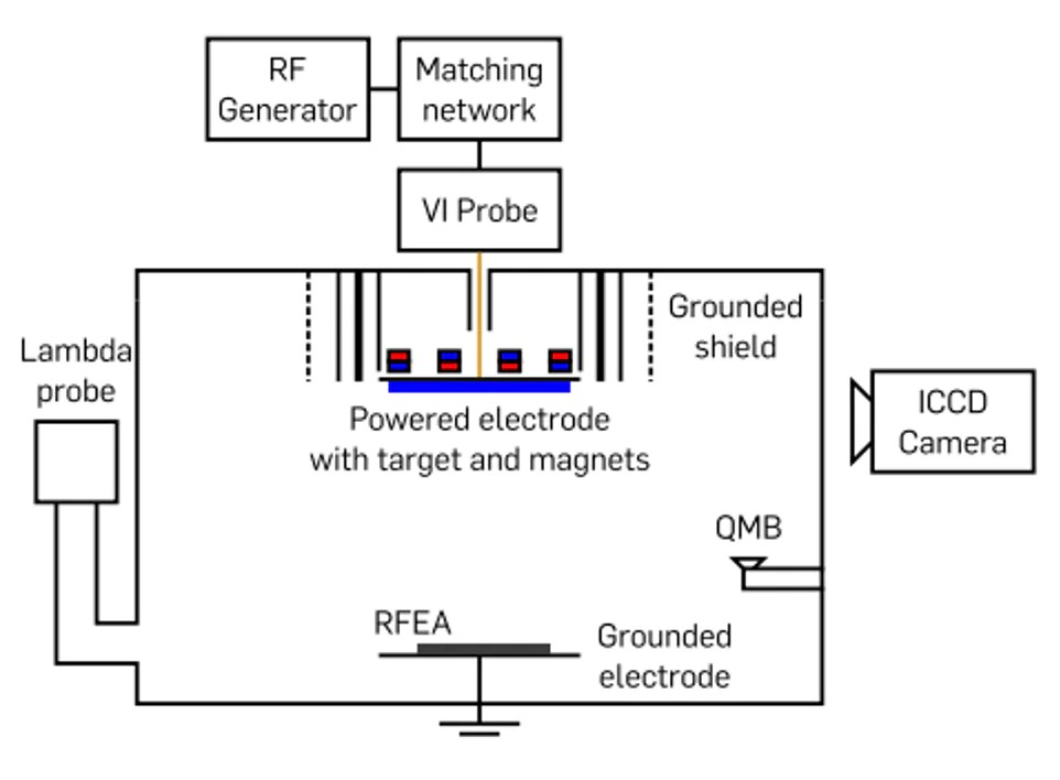
Because the mass of electrons is much smaller than that of ions, their movement speed is much faster than that of ions. When positive ions hit the target surface, their energy is transferred to the target atoms, so that the target atoms gain enough energy to sputter out from the target surface. The sputtered target atoms fly freely in the vacuum chamber, and some atoms reach the substrate surface and deposit. As time accumulates, a thin film gradually forms on the substrate surface.
RF Sputtering Working Process
Vacuum preparation: Place the substrate to be deposited on the substrate holder in the vacuum chamber to ensure that the substrate surface is clean and free of impurities and contaminants. Close the vacuum chamber, start the vacuum pump group, and pump the vacuum chamber to the required vacuum degree through mechanical pumps and molecular pumps.
Gas introduction: Introduce an appropriate amount of inert gas (argon) into the vacuum chamber through a mass flow controller (MFC). Generally speaking, the gas flow rate is between a few sccm (standard cubic centimeters per minute) and tens of sccm.
RF power starting: Turn on the RF power and set appropriate RF power, frequency and other parameters. The size of the RF power directly affects the density of the plasma and the energy of the ions, which in turn affects the sputtering rate and film quality.
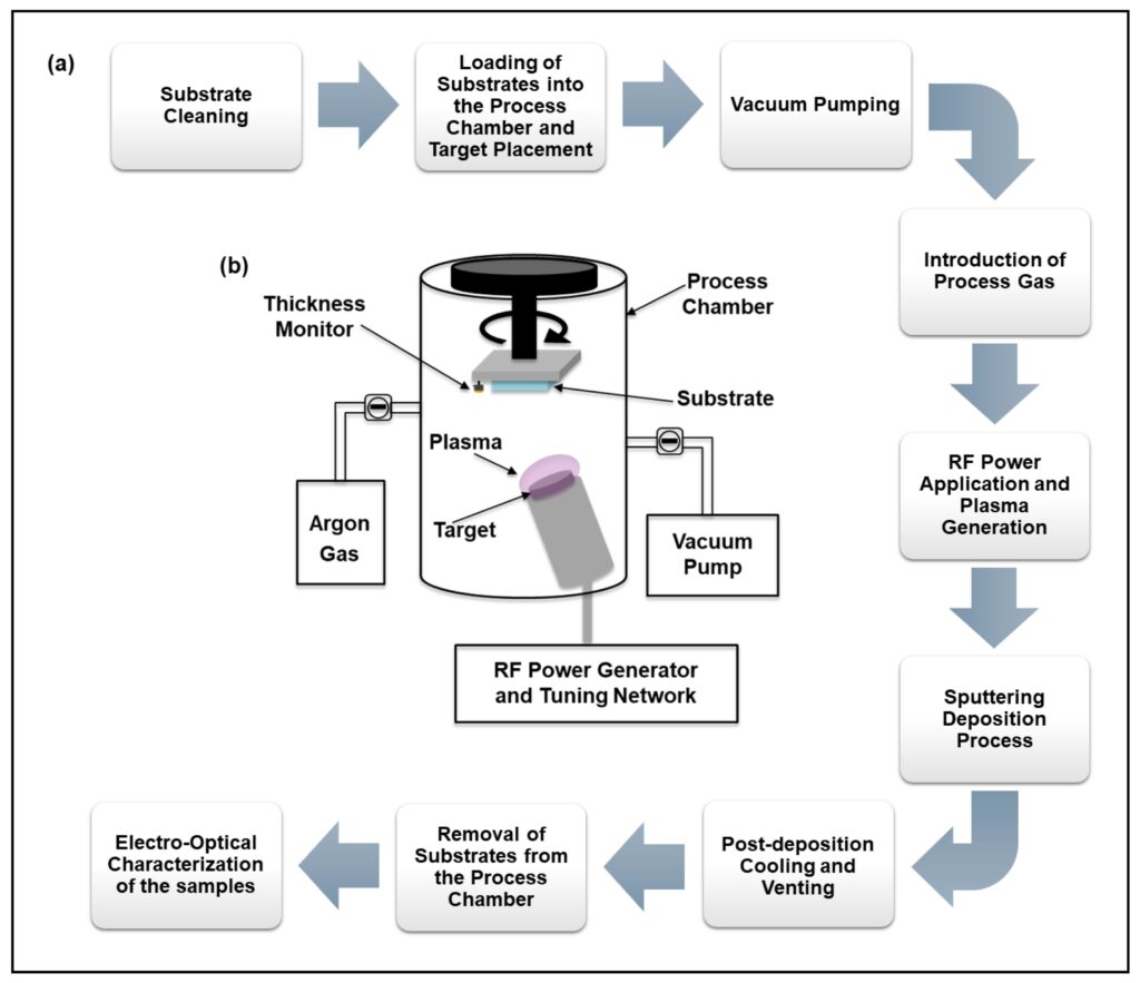
Deposition and monitoring: As the sputtering time increases, the film on the substrate surface gradually thickens. The film growth process is monitored by a variety of methods, such as quartz crystal microbalance (QCM), optical emission spectroscopy (OES), etc.
End: First turn off the RF power supply and stop sputtering. Then continue to maintain the vacuum for a while to allow the plasma and residual gas in the vacuum chamber to be fully discharged. Finally, the vacuum chamber returns to normal pressure and the substrate with the film deposited is taken out.
RF Voltage Calculation
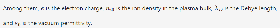
RF voltage is an important parameter, which is closely related to the generation of plasma, the energy of ions and the sputtering effect. The RF voltage is adjusted according to different target materials, gas pressure, sputtering rate and other requirements. However, accurate calculation of RF voltage in RF sputtering is a complex process, involving knowledge in multiple fields such as plasma physics and electromagnetics. From the basic principle, the RF voltage is closely related to the characteristics of the plasma sheath. The sheath voltage (Vs) is an important component of the RF voltage. It determines the energy of ions bombarding the target surface. Some simplified models are used to estimate the sheath voltage. For example, in the RF capacitively coupled plasma (CCP) model, assuming that the plasma is electrically neutral and the ion motion in the sheath satisfies the Boltzmann distribution, the following approximate formula for the sheath voltage can be obtained:

However, actual RF sputtering is far more complicated than this simple model. It is also necessary to consider the gas pressure, the characteristics of the target and substrate, the characteristics of the RF power supply, etc. In practice, an oscilloscope and other equipment are used to measure the output voltage and current waveform of the RF power supply, and a power meter is used to measure the RF power. Then, the RF voltage is adjusted according to the sputtering effect (such as sputtering rate, film quality, etc.) to achieve the best sputtering conditions. At the same time, some empirical formulas and previous research results can also be used to estimate the initial RF voltage to reduce the blindness of the experiment.
Why is the frequency 13.56MHz?
In RF sputtering technology, the frequency of 13.56MHz is widely used internationally. This choice is not accidental, but a comprehensive consideration of many factors:
13.56MHz is within the industrial, scientific and medical (ISM) frequency band. For a long time, 13.56MHz RF technology has been widely used and deeply studied in various fields, and the relevant equipment technology has been very mature. This frequency band is divided by the International Telecommunication Union (ITU) for non-communication purposes, and is specifically used for industrial, scientific research, medical equipment, and radio frequency identification (RFID) applications. Effectively avoid interference with conventional communication frequencies (such as radio, television, mobile communications, etc.). From the perspective of plasma physics, the frequency of 13.56MHz can effectively excite and maintain plasma. At this frequency, the RF electric field can enable the electrons in the plasma to obtain sufficient energy to collide with the working gas molecules (such as argon) and ionize them. The use of a unified 13.56MHz frequency facilitates the interchangeability and compatibility between RF sputtering equipment produced by different manufacturers.

RF Sputtering vs. DC Sputtering
DC sputtering technology can only be used for conductive materials, and is helpless against insulating materials such as ceramics and polymers. When a DC voltage is applied to an insulating target, the surface of the target will form a “charge shield” due to charge accumulation, causing the electric field strength to decay rapidly and sputtering to be difficult to sustain. RF sputtering has become the key to breaking through this dilemma.
| Comparison | RF Sputtering | DC Sputtering |
| Power | RF power source, usually with a frequency of 13.56 MHz, and an alternating electric field. | DC power source, and a constant electric field. |
| Target | Can sputter almost any material, including conductors, semiconductors, and insulators. | Mainly applicable to conductive targets, and it is difficult to sputter insulating targets. |
| Charge | Through the alternating electric field, the positive charges on the target surface are neutralized in the positive half-cycle, and sputtering is realized in the negative half-cycle, avoiding abnormal discharge caused by charge accumulation. | On insulating targets, the bombardment of positive ions will cause positive charges to accumulate on the target surface, resulting in a decrease in the electric field, the extinction of glow discharge, and the stop of sputtering. |
| Plasma | The RF electric field makes it easier for electrons to oscillate in the electric field, absorb energy and collide with gas molecules for ionization. The generation and maintenance of plasma are relatively easy, and the working gas pressure can be as low as about 1 Pa. | A relatively high voltage is required to generate secondary electrons to maintain discharge, and the working gas pressure is generally about 10 Pa. |
| Sputtering Rate | For some materials, the sputtering rate is relatively low, but a relatively high deposition rate can also be achieved under optimized conditions. | When sputtering conductive targets, the sputtering rate is usually relatively high. |
| Film Quality | Can obtain dense, high-purity films with firm adhesion to the substrate, especially when depositing insulating material films, the advantage is obvious. | High-quality films can also be obtained under suitable conditions, but there are limitations in the deposition of insulating material films. |
| Equipment Cost | Requires complex equipment such as RF power sources and matching networks, and the cost is relatively high. | The equipment is relatively simple and the cost is relatively low. |
| Application Fields | Widely used in semiconductor, optical, electronic, biomedical and other fields for preparing various functional films, such as oxide, nitride, carbide films, etc. | Mainly used in the preparation of metal films, in some fields with less demand for insulating material films. |
RF sputtering technology uses high-frequency alternating electric fields to cleverly solve the problem of charge accumulation on the surface of insulating targets, making sputtering technology widely applicable to various materials and greatly expanding its application range. Wstitanium lists 30 insulating sputtering targets.
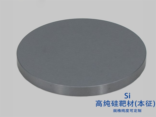
Silicon (Si) Sputtering Target
The chemical properties of silicon are relatively stable. It is not easy to react chemically with other substances during sputtering, which can ensure the purity of the film. Secondly, silicon film has good crystallinity. Silicon targets are often used to prepare silicon-based semiconductor devices, such as solar cells and thin film transistors. However, the sputtering rate of silicon is relatively low.
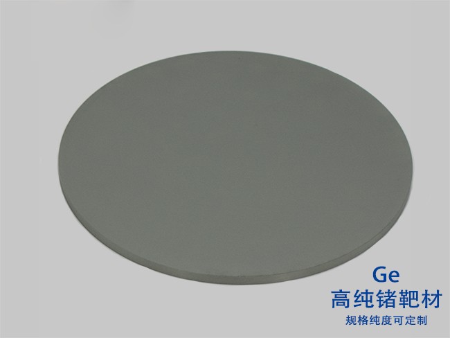
Ge Sputtering Target
The advantages of germanium are high electron mobility and good optical absorption characteristics. It is widely used in infrared optical devices and optoelectronic devices. Germanium film is used to prepare germanium-based transistors, infrared detectors, etc. Germanium easily reacts with oxygen and other substances to form germanium oxide, which affects the performance of the film.
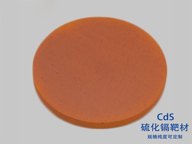
Cadmium sulfide (CdS)
Cadmium sulfide is widely used in solar cells, light emitting diodes and photodetectors. Cadmium sulfide thin films effectively improve the conversion efficiency of solar cells. In RF sputtering, the sputtering of cadmium sulfide targets needs to pay attention to the stoichiometric ratio control of the material. In addition, the toxicity of cadmium sulfide also needs to be considered.
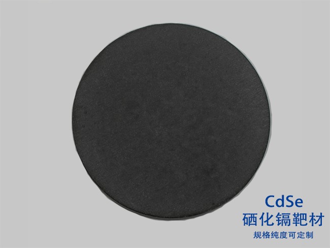
Cadmium selenide (CdSe)
Cadmium selenide has a wide range of applications in the fields of photoelectric conversion, optical storage and biomedicine. CdSe thin films are used to prepare CdSe-based solar cells, photodetectors and biosensors. In RF sputtering, attention should be paid to crystallinity and optical properties. In addition, the toxicity of CdSe is also a concern.
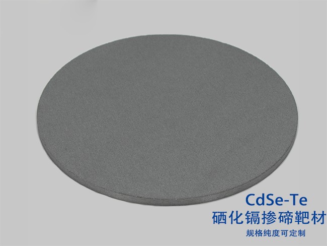
Cadmium telluride (CdTe)
Cadmium telluride has a wide range of applications in the field of solar cells. It is the core absorption layer material of CdTe thin film solar cells. In RF sputtering, the sputtering of CdTe targets needs to pay attention to the stoichiometric ratio and crystallinity of the materials. In addition, the toxicity of CdTe is also a concern.
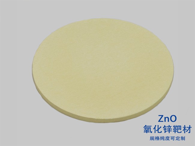
Zinc oxide (ZnO)
Zinc oxide is an important wide bandgap semiconductor material with good optical, electrical and piezoelectric properties. It is widely used in transparent conductive films, UV detectors, light-emitting diodes and piezoelectric devices. In RF sputtering, attention should be paid to doping and crystal orientation.
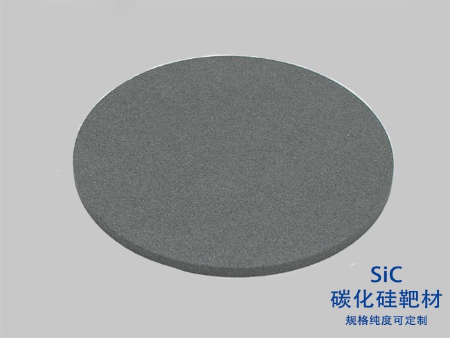
Silicon Carbide (SiC)
Silicon carbide has excellent electrical, thermal and chemical stability and is used in high-temperature, high-frequency, high-power electronic devices and nuclear radiation detection. Silicon carbide, such as cubic phase (3C-SiC), hexagonal phase (4H-SiC, 6H-SiC), etc., has different electrical and optical properties. Silicon carbide-based devices are widely used in aerospace, energy and automobiles.
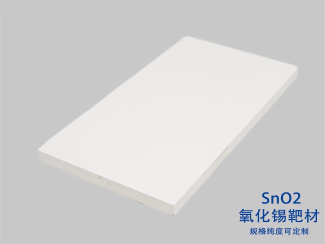
Tin oxide (SnO₂)
Tin oxide has good optical, electrical and chemical stability and is widely used in transparent conductive films, gas sensors and lithium battery electrodes. The electrical properties of tin oxide can be regulated by doping elements such as fluorine and antimony to obtain highly conductive transparent conductive films.
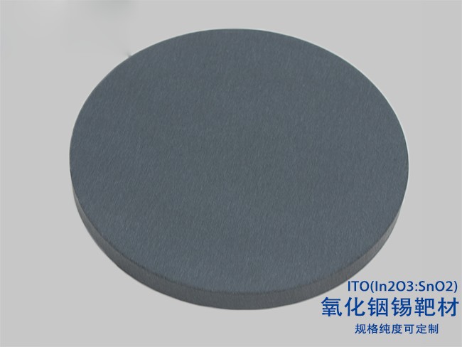
Indium tin oxide (ITO)
Indium tin oxide is a transparent conductive oxide material with excellent optical and electrical properties. It is widely used in flat panel displays, solar cells, touch screens and electromagnetic shielding. Usually the content of indium oxide is about 90% and the content of tin oxide is about 10%.
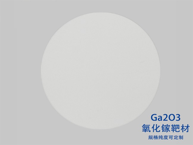
Gallium oxide (Ga₂O₃)
Gallium oxide has extremely high breakdown electric field and good thermal stability, and has broad application prospects in power electronic devices and ultraviolet detectors. Gallium oxide has a variety of crystal structures, such as β-Ga₂O₃, α-Ga₂O₃, etc., among which β-Ga₂O₃ is the most stable and has excellent electrical properties. Gallium oxide-based power electronic devices have advantages such as low on-resistance and high switching speed.
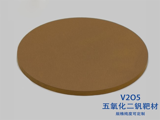
Vanadium oxide (V₂O5)
Vanadium oxide has unique metal-insulator phase transition properties. Vanadium oxide-based smart windows have high transmittance at low temperatures, allowing sunlight to enter the room and increase the indoor temperature. At high temperatures, its transmittance decreases, blocking sunlight from entering the room and reducing the indoor temperature.
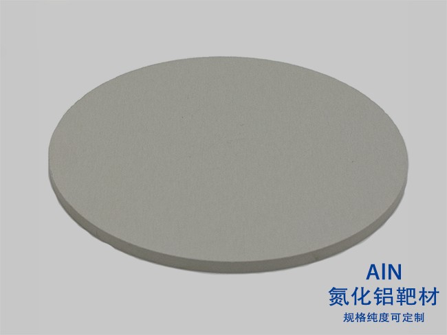
Aluminum Nitride (AlN)
Aluminum nitride has excellent electrical, optical and piezoelectric properties and is widely used in high-frequency electronic devices, surface acoustic wave devices and ultraviolet detectors. Aluminum nitride has a hexagonal wurtzite structure, and its piezoelectric properties make it widely used in surface acoustic wave devices. Communications, radar, electronic warfare, etc.
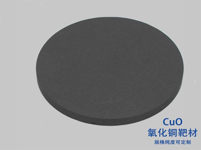
Copper Oxide (CuO)
Copper oxide has good optical, electrical and catalytic properties and is widely used in gas sensors, photoelectrochemical cells and photocatalysis. Copper oxide is widely used in environmental monitoring, industrial safety and medical diagnosis in the field of gas sensors.
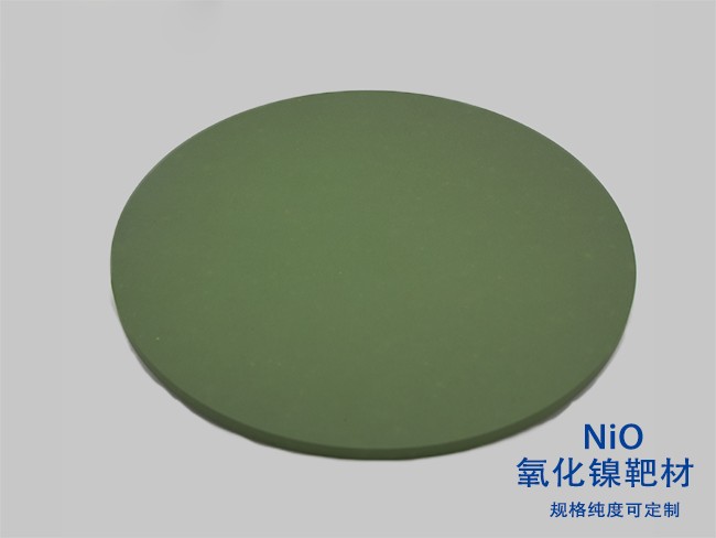
Nickel Oxide (NiO)
Nickel oxide is an important p-type semiconductor material with good optical, electrical and magnetic properties. It is widely used in electrochromic devices, sensors and battery electrodes. In addition, the electrochromic properties of nickel oxide make it widely used in electrochromic devices.
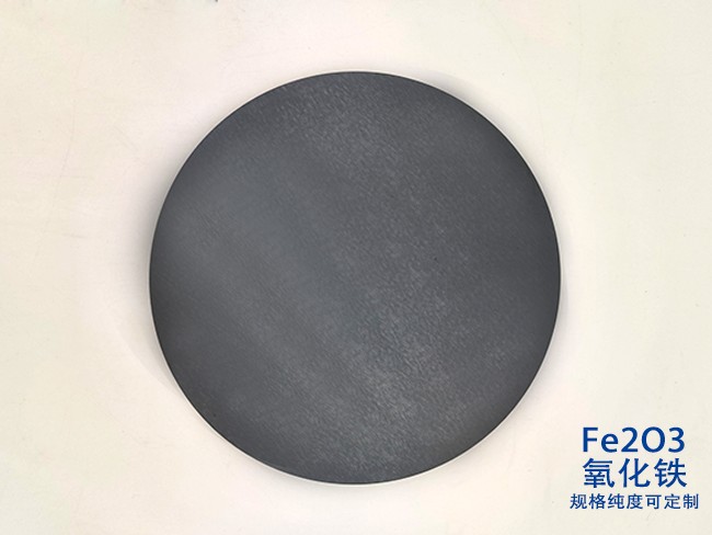
Iron Oxide (Fe₂O₃)
Iron oxide is an important n-type semiconductor material with a wide range of applications in photocatalysis, gas sensors and magnetic recording. The photocatalytic properties of iron oxide are used to degrade organic pollutants, decompose water to produce hydrogen and reduce carbon dioxide.
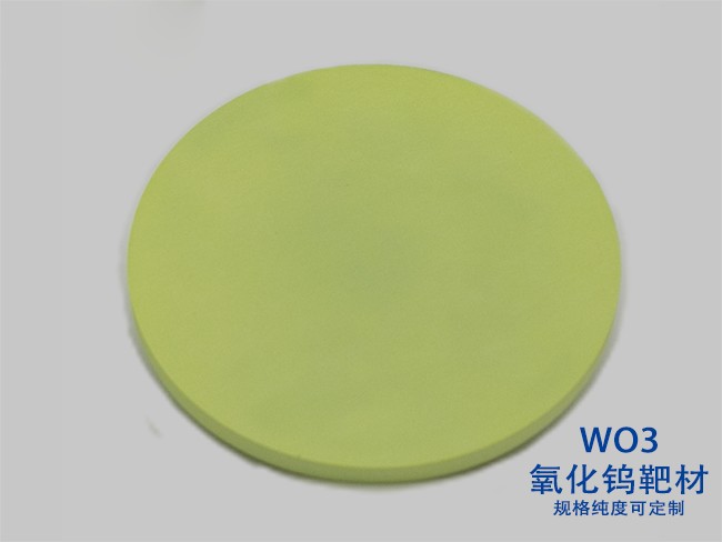
Tungsten oxide (WO₃)
Tungsten oxide has good optical, electrical and catalytic properties, and is widely used in electrochromic devices, gas sensors and photocatalysis. Tungsten oxide has a variety of crystal structures, such as monoclinic phase, orthorhombic phase, tetragonal phase, etc. Tungsten oxide is widely used in smart windows, displays and automotive rearview mirrors.
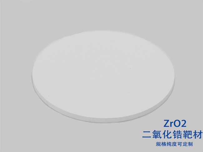
Zirconium oxide (ZrO₂)
Zirconium oxide is an insulator material with high chemical stability, thermal stability and mechanical strength. It is widely used in high-temperature coatings, solid oxide fuel cells and oxygen sensors. In addition, the high oxygen ion conductivity of zirconium oxide makes it have broad application prospects in solid oxide fuel cells and oxygen sensors.

Aluminum oxide (Al₂O₃)
Aluminum oxide has high chemical stability, thermal stability and electrical insulation properties, and is widely used in microelectronic packaging, optical coatings and wear-resistant coatings. Aluminum oxide-based packaging materials have high electrical insulation properties and good thermal conductivity, effectively protecting chips and dissipating heat.
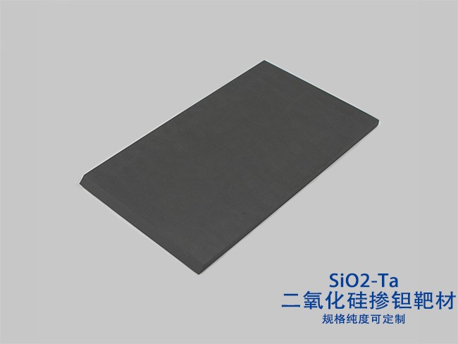
Silicon oxide (SiO₂)
Silicon oxide has good chemical stability, thermal stability and electrical insulation properties, and is widely used in microelectronics, optics and semiconductors. Silicon oxide film effectively isolates different circuit components to ensure the reliability and stability of the chip.
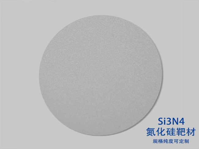
Silicon nitride (Si₃N₄)
Silicon nitride has high hardness, wear resistance, chemical stability and thermal stability, and is widely used in microelectronics, optics and machinery. In addition, the high hardness and wear resistance of silicon nitride make it have broad application prospects in the mechanical field.
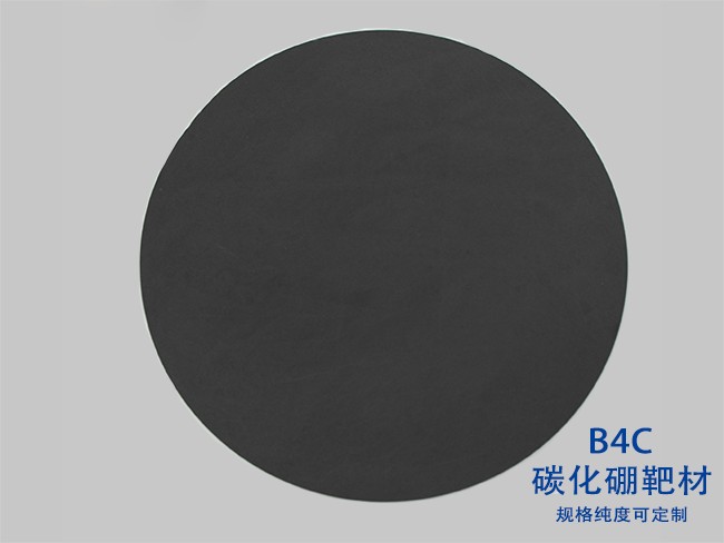
Boron carbide (B₄C)
Boron carbide has extremely high hardness, wear resistance and neutron absorption ability, and is widely used in the nuclear industry, aerospace and wear-resistant coatings. Boron carbide is used to prepare control rods and shielding materials to effectively control the progress of nuclear reactions.
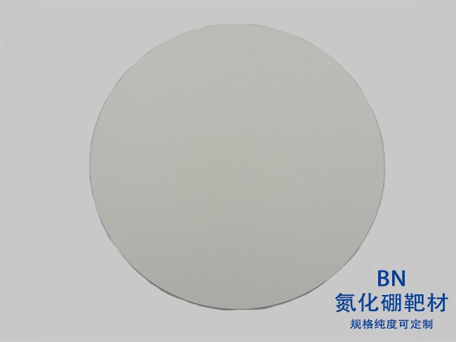
Boron nitride (BN)
Boron nitride has a graphite-like layered structure, high thermal conductivity, good electrical insulation and chemical stability, and is widely used in electronic packaging, heat dissipation materials and high-temperature lubricants. Boron nitride effectively dissipates the heat generated by electronic devices. The preparation cost of boron nitride film is relatively high.
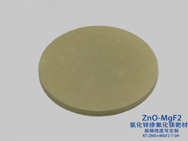
Magnesium fluoride (MgF₂)
Magnesium fluoride has good optical properties, chemical stability and electrical insulation properties, and is widely used in optical coatings, ultraviolet detectors and electronic devices. Magnesium fluoride film can be used to prepare anti-reflection film, anti-reflection film and protective film, etc., to improve the performance and reliability of optical devices.
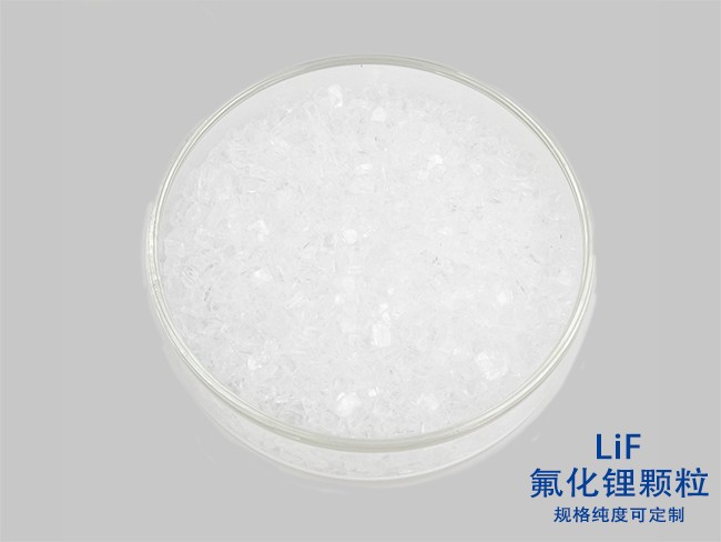
Lithium fluoride (LiF)
Lithium fluoride has good optical properties, chemical stability and ionic conductivity, and is widely used in optical coatings, lithium-ion batteries and nuclear industry. Lithium fluoride achieves efficient lithium ion transmission and improves battery performance. Lithium fluoride film has high transmittance and low absorption loss for ultraviolet light.
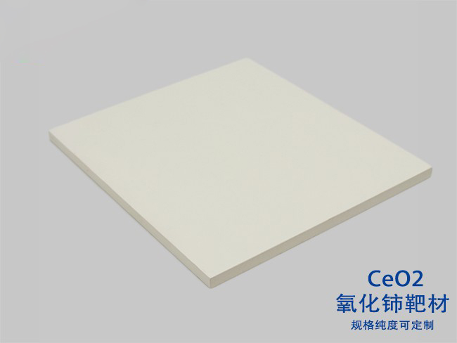
Cerium oxide (CeO₂)
Cerium oxide has a fluorite structure, a melting point of about 2600℃, and a density of 7.13g/cm³. It has excellent oxygen ion conductivity (especially at high temperatures), chemical stability, and optical properties. Cerium oxide films are often used as electrolytes or electrolyte additives. Cerium oxide is insulating.
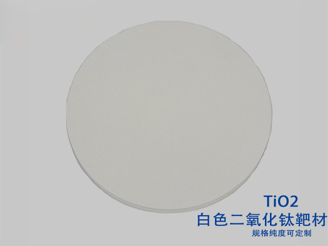
Titanium dioxide (TiO₂)
Titanium dioxide has three crystal forms: anatase phase, rutile phase, and brookite phase, among which anatase phase and rutile phase have good photocatalytic properties. Its melting point is about 1843℃ and its density is 4.26g/cm³. Titanium dioxide film has a high refractive index and good chemical stability.
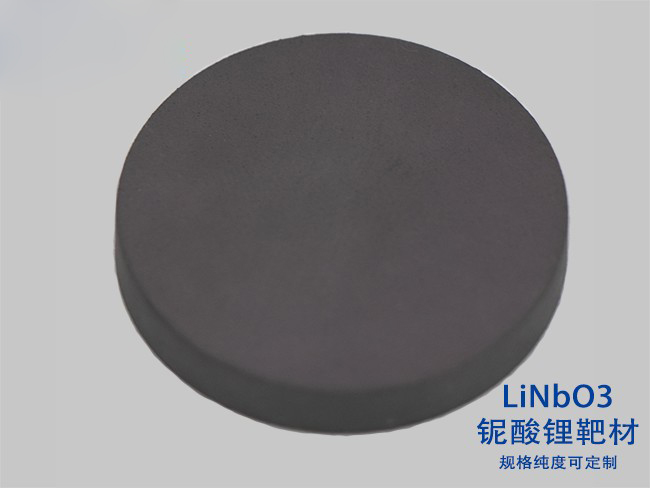
Lithium niobate (LiNbO₃)
Lithium niobate has a trigonal crystal structure, a melting point of about 1250°C, and a density of 4.64g/cm³. It has excellent piezoelectric properties (high electromechanical coupling coefficient), electro-optic effect (refractive index changes with applied electric field) and nonlinear optical properties.
Advantages of RF Sputtering
RF sputtering technology has many significant advantages in the field of thin film preparation due to its unique working principle and performance characteristics:
Wide range of materials
This is one of the most prominent advantages of RF sputtering. Including various metals, alloys, ceramics, compounds, etc., which greatly expands the range of choices.
High film quality
RF sputtering can produce films with high density, good uniformity and high purity. During sputtering, atoms can better diffuse and arrange when deposited on the substrate surface to form a densely structured film.
Strong controllability
Key parameters in the RF sputtering process, such as RF power, sputtering gas pressure, gas flow, substrate temperature, target-substrate distance, etc., can be precisely controlled.
Achieve large-area uniform deposition
RF sputtering is suitable for the structure of large-area substrates and can produce films with good uniformity on large-area substrates. This advantage makes it have important application value in flat-panel displays, solar cells, large-area optical coatings, etc.
Strong adhesion to substrate
In RF sputtering, when the sputtered high-energy atoms are deposited on the substrate surface, they will interact strongly with the substrate and may even form interface alloys or compounds, thereby significantly improving the adhesion between the film and the substrate.
Multilayer composite film
RF sputtering can produce multilayer composite films by replacing different targets or changing the gas composition during sputtering. Multilayer optical film systems achieve specific optical functions (high reflection, narrowband filtering, etc.). Multilayer metal-insulating layer films can be used to prepare magnetoresistance devices, etc.
Disadvantages of RF Sputtering
Although RF sputtering has many advantages, it also has some shortcomings that need to be considered and overcome in practical applications:
High equipment cost
RF sputtering systems require equipment such as RF power supplies and matching networks. The manufacturing and maintenance costs of these devices are relatively high. In contrast, DC sputtering equipment is simpler and cheaper. This makes the initial investment in RF sputtering equipment relatively large.
Relatively low sputtering rate
For many materials, especially insulating materials, the rate of RF sputtering is usually lower than the sputtering rate of DC sputtering on conductive targets. The acceleration and energy transfer efficiency of ions in the sheath are relatively low, and the sputtering yield of insulating targets is usually not high.
Low target material utilization
Due to factors such as the distribution of plasma and the directionality of ion bombardment, the surface of the target material is prone to uneven “etching”, forming “target poisoning” or “target surface depression”, resulting in low target material utilization.
RF interference
When the RF power supply is working, electromagnetic radiation is generated, which may interfere with surrounding electronic equipment and measuring instruments. In order to reduce this interference, special shielding measures need to be taken.
Applications of RF Sputtering
The advantages of RF sputtering technology have been fully demonstrated. In the field of semiconductor manufacturing, it provides key technology for the preparation of high-performance chips and integrated circuits. In the field of optics, high-quality optical films prepared by RF sputtering have significantly improved the performance of optical devices and met the high requirements of optical systems in different application scenarios. In the fields of machinery, aerospace, etc., the protective coating prepared by RF sputtering enhances the wear resistance, corrosion resistance and high temperature resistance of the material surface, prolongs the service life of parts and components, and improves the ability of equipment to work in extreme environments.
Semiconductor
In semiconductor chip manufacturing, RF sputtering is one of the key technologies for preparing various functional films. For example, silicon dioxide (SiO₂) and silicon nitride (Si₃N₄) films for insulating layers, aluminum (Al) and copper (Cu) films for metal interconnect layers, titanium (Ti) and tantalum (Ta) films for diffusion barrier layers, etc. The quality of these films directly affects the performance, reliability and integration of the chip. RF sputtering technology can meet the strict requirements of the semiconductor industry for film thickness, uniformity, purity, etc.
Optics
RF sputtering plays an important role in the preparation of optical films. It is used to manufacture various optical components such as anti-reflection films, high-reflection films, filters, and spectroscopes. For example, a multilayer anti-reflection film of alternating silicon dioxide (SiO₂) and titanium dioxide (TiO₂) is deposited on the surface of eyeglass lenses and camera lenses to significantly improve the light transmittance of the lens. The use of highly reflective films (such as metal silver films or multilayer dielectric films) in laser resonators can improve the output efficiency of lasers. In addition, RF sputtering can also prepare special optical films for infrared detection, optical communications, and other fields.
Electronics
In the manufacture of electronic devices, RF sputtering technology is used to prepare various electrodes, sensor films, piezoelectric films, etc. For example, in flat panel displays (LCD, OLED), the transparent conductive film of indium tin oxide (ITO) prepared by RF sputtering is used as an electrode, which has high transmittance and good conductivity; in the field of sensors, the piezoelectric and gas-sensitive properties of zinc oxide (ZnO) and aluminum nitride (AlN) films can be used to manufacture pressure sensors, gas sensors, etc.; in piezoelectric devices, the application of lithium niobate (LiNbO₃) and lithium tantalate (LiTaO₃) films gives them excellent electroacoustic conversion performance.

Surface Modification and Protection
RF sputtering technology can be used to modify and protect the surface of materials, improving the wear resistance, corrosion resistance, high temperature resistance and other properties of materials. For example, sputtering hard films such as titanium nitride (TiN) and titanium carbide (TiC) on the surface of tools and molds can significantly improve their service life; depositing zirconium oxide (ZrO₂) thermal barrier coatings on the surface of aerospace parts to reduce the heating temperature of the parts and improve their high temperature resistance; sputtering corrosion-resistant films such as aluminum oxide (Al₂O₃) and silicon dioxide (SiO₂) on the surface of metal materials to prevent metal corrosion.
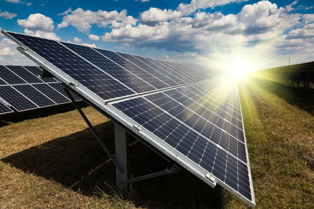
New Energy
In solar cell manufacturing, RF sputtering is used to prepare various functional films, such as copper indium gallium selenide (CIGS), cadmium telluride (CdTe) and other absorption layer films. Transparent conductive films such as zinc oxide (ZnO) and indium tin oxide (ITO). Anti-reflection films and passivation films such as silicon nitride (Si₃N₄). These films are the key to improving the photoelectric conversion efficiency of solar cells. In the field of lithium-ion batteries, RF sputtering is used to prepare electrode material films and diaphragm coatings to improve the performance and safety of batteries.
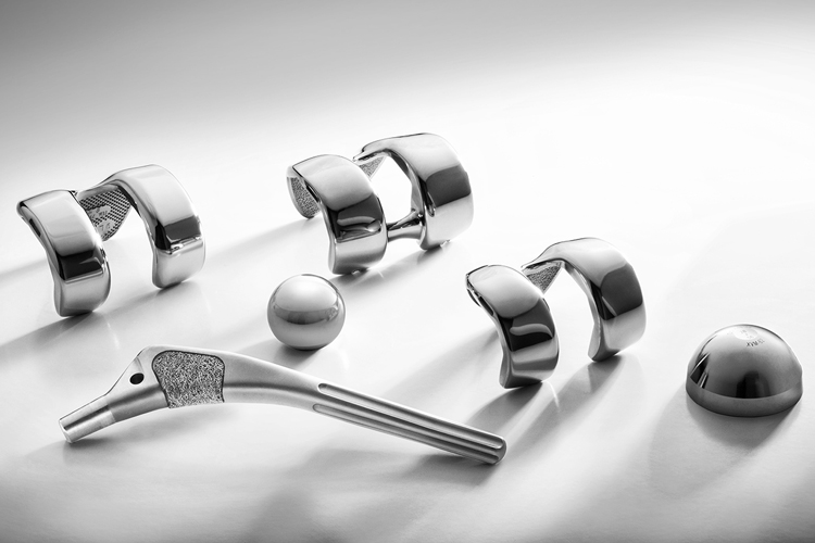
Biomedicine
RF sputtering technology is also increasingly used in the biomedical field. Taking advantage of its ability to prepare biocompatible films, thin films such as titanium (Ti), titanium nitride (TiN), and zirconium oxide (ZrO₂) are deposited on the surface of medical devices (such as artificial joints and dental implants) to improve the biocompatibility, wear resistance and corrosion resistance of the devices, and reduce the body’s rejection of foreign bodies. In addition, biosensor films with special functions prepared by RF sputtering can be used for the detection and diagnosis of biological molecules.
Conclusion
This article comprehensively explains the relevant knowledge of RF sputtering, including its definition, working principle and process – plasma is excited by RF electric field, ions bombard the target material to sputter out atoms and deposit on the substrate to form a thin film. The complexity of RF voltage calculation and influencing factors are analyzed. The reasons why the 13.56MHz frequency is widely used are explained, such as avoiding communication interference, high plasma excitation efficiency, and mature equipment. By comparing with DC sputtering, the advantages of RF sputtering in material applicability are highlighted. 30 commonly used insulating sputtering targets are introduced in detail. Each material is explained from the perspective of characteristics, application and sputtering characteristics. At the same time, the advantages of RF sputtering are summarized, such as wide range of material applications, high film quality, strong parameter controllability, etc., and its disadvantages such as high equipment cost and low sputtering rate are also pointed out. Finally, its wide application in various fields is outlined.