Atmospheric Pressure Chemical Vapor Deposition
APCVD plays an indispensable role in industries such as integrated circuit manufacturing, solar cells, and flat panel displays, becoming a key method for manufacturing various thin films. In-depth research and comprehensive understanding of APCVD technology are crucial for the development of thin films.
- Good Film Uniformity
- Higher Film Deposition Rate
- Strong Film-Substrate Bonding
- Compatible With Conductive Materials
Everything You Should Know About APCVD
Atmospheric pressure chemical vapor deposition (APCVD) technology, with its core advantages of “low cost, high efficiency, and wide adaptability”, has become an indispensable key technology in the field of thin film deposition. It has achieved large-scale application in fields such as solar cells, architectural glass, tool coatings, and flexible electronics, providing important support for cost reduction and efficiency improvement in related industries.
What is APCVD?
Atmospheric pressure chemical vapor deposition (APCVD) refers to chemical vapor deposition performed at atmospheric pressure. Unlike other chemical vapor deposition techniques, such as low-pressure chemical vapor deposition (LPCVD) and plasma-enhanced chemical vapor deposition (PECVD), APCVD does not require complex vacuum equipment to maintain the low-pressure environment. Instead, gaseous precursors are delivered directly to the reaction chamber at atmospheric pressure, where they chemically react on the substrate surface to deposit a solid film. This makes the technology more cost-effective and easier to scale for industrial applications.

The family of chemical vapor deposition technologies includes, in addition to APCVD, low-pressure chemical vapor deposition (LPCVD), plasma-enhanced chemical vapor deposition (PECVD), and metal-organic chemical vapor deposition (MOCVD). LPCVD reduces the reaction pressure, minimizing gas-phase reactions and improving film uniformity and quality, but it suffers from a relatively low deposition rate. PECVD utilizes plasma to enhance reactivity, enabling thin-film deposition at lower temperatures, making it suitable for temperature-sensitive materials and devices. However, the equipment cost is relatively high. APCVD, on the other hand, is distinguished by its operation at atmospheric pressure, simple equipment, and fast deposition rates, though it lags slightly behind LPCVD and PECVD in terms of film uniformity. Each of these different CVD technologies has its own advantages and disadvantages. In practical applications, the appropriate technology should be selected based on specific process requirements and material properties. They complement each other and collectively promote the development and application of thin-film deposition technology.
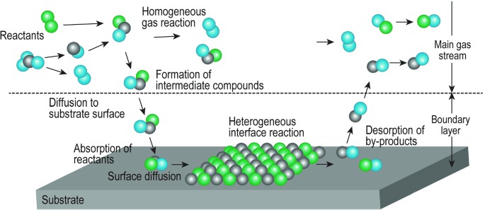
APCVD Process
The basic principle of APCVD is that gaseous precursors enter a reaction chamber at atmospheric pressure, undergo a chemical reaction on the substrate surface, and form a solid thin film material that is then deposited on the substrate. The reaction process primarily involves the following steps:
- 1. Reaction Gas Delivery
A gaseous precursor containing the film’s constituent elements (e.g., silane SiH₄ for silicon thin film deposition) and a carrier gas (e.g., hydrogen H₂, nitrogen N₂, etc.) are introduced into the reaction chamber in a specific ratio via a gas delivery system. The carrier gas helps evenly distribute the precursor within the reaction chamber and controls the concentration and flow rate of the reaction gas.
- 2. Gas Diffusion and Adsorption
The gaseous precursor entering the reaction chamber is transported to the substrate surface by diffusion at atmospheric pressure and adsorbed onto active sites on the substrate surface. Because the reaction is carried out at atmospheric pressure, the mean free path of the gas molecules is relatively short. This somewhat affects the uniformity of gas diffusion, but also results in a relatively high reaction rate.
- 3. Chemical Reaction
Precursor molecules adsorbed on the substrate surface undergo a chemical reaction under certain temperature conditions (typically 400-800°C for APCVD), decomposing or reacting with other molecules to form a solid thin film material. For example, silane (SiH₄) decomposes into silicon atoms (Si) and hydrogen (H₂) at high temperatures. The silicon atoms gradually deposit on the substrate surface to form a silicon thin film.
- 4. Thin Film Growth
The solid thin film atoms or molecules generated by the chemical reaction continuously aggregate and crystallize on the substrate surface, gradually forming a continuous thin film. As the reaction continues, the film thickness increases until the desired thickness is reached.
- 5. Byproduct Exhaust
Byproducts produced in the chemical reaction (such as hydrogen H₂ from the decomposition of silane) desorb from the substrate surface in gaseous form and are discharged from the reaction chamber through the exhaust system.
Reaction Rate
In APCVD, the reaction rate is influenced by a variety of factors, including reaction temperature, reactant gas concentration, and substrate surface activity. According to the Arrhenius equation: k = A * exp (-Ea / RT), where k is the reaction rate constant, A is the pre-exponential factor, Ea is the reaction activation energy, R is the gas constant, and T is the absolute temperature. This equation shows that the reaction temperature, T, has a significant impact on the reaction rate. Increasing the temperature increases the reaction rate constant, k, and the reaction rate accelerates. Furthermore, increasing the reactant gas concentration also increases the reaction rate because more reactant molecules are available for reaction. Furthermore, the number and properties of active sites on the substrate surface also influence the reaction rate and film growth quality. More active sites promote precursor adsorption and facilitate the reaction.
APCVD-Produced Thin Films
As a mature and highly promising thin-film deposition technology, APCVD has enabled the large-scale production of a wide range of thin films (including semiconductors, oxides, nitrides, metals, and compound semiconductors) in the semiconductor, photovoltaic, optical, and electronics fields. Here are 30 representative examples.
- SiC Film
SiC film features high hardness, chemical stability, thermal conductivity, and a wide bandgap. It is used in high-temperature electronic devices, power components, and wear-resistant coatings. Silane and methane are commonly used as precursors in its preparation, with the reaction temperature typically ranging from 1000 to 1500°C.
- BaTiO₃ Film
BaTiO₃ film exhibits a variety of excellent properties, including ferroelectric, piezoelectric, and dielectric properties. It is widely used in electronic devices such as capacitors, sensors, and memory devices. Metal-organic compounds are typically used as precursors, and in APCVD, the reaction temperature is typically between 600°C and 900°C.
- Pb (ZrₓTi₁₋ₓ) O₃ Film
Pb (ZrₓTi₁₋ₓ) O₃ films are commonly used in the production of piezoelectric sensors, actuators, and piezoelectric components in microelectromechanical systems (MEMS). The film’s piezoelectric properties are adjusted by controlling the ratio of zirconium to titanium during fabrication, typically at temperatures between 500 and 800°C.
- ZnO Film
ZnO film has excellent optical properties (strong absorption in the ultraviolet region), piezoelectric properties, and semiconductor characteristics. It has applications in UV detectors, transparent conductive electrodes, and surface acoustic wave devices. Diethylzinc and oxygen are commonly used as precursors, and the reaction temperature is generally between 300 and 600°C.
- In₂O₃:Sn Film
ITO film is an important transparent conductive oxide film with high visible light transmittance and good conductivity. As a transparent conductive electrode, it is widely used in liquid crystal displays (LCDs), organic light-emitting diodes (OLEDs), and touch screens. Organic compounds of indium and tin are used as precursors, and the reaction temperature is between 400 and 800°C.
- CdS Film
CdS film has a direct band gap and is a commonly used semiconductor material. It is used as a window layer in solar cells to improve light absorption efficiency. It can also be used in photodetectors. Dimethylcadmium and hydrogen sulfide are commonly used as precursors, and the reaction temperature is generally between 300 and 500°C.
- CdTe Film
CdTe film is an important photovoltaic material with a high light absorption coefficient and a suitable band gap. It is commonly used in the production of cadmium telluride solar cells and plays a key role in the photovoltaic industry. Dimethylcadmium and hydrogen telluride are commonly used as precursors in its preparation, and the reaction temperature is generally between 400 and 600°C.
- TiN Film
TiN film features high hardness, high chemical stability, good conductivity, and a golden appearance. It improves the wear resistance and cutting performance of cutting tools; it can be used as a gold-like coating, a diffusion barrier, and an electrode material. Titanium tetrachloride and ammonia are commonly used as precursors, and the reaction temperature is generally between 800 and 1000°C.
- TiC Film
TiC film features high hardness, a high melting point, and excellent wear resistance. It is used in the production of surface coatings for wear-resistant parts, significantly improving the material’s wear resistance and lifespan. Titanium tetrachloride and methane are commonly used as precursors in its preparation, with the reaction temperature generally ranging from 1000-1200°C.
- TiB₂ Film
TiB₂ film features high hardness, high conductivity, and excellent chemical stability. It is used in cutting tool coatings, electrode materials, and wear-resistant coatings. Titanium tetrachloride and borane are commonly used as precursors, and the reaction temperature is generally between 1000 and 1300°C.
- MoSi₂ Film
MoSi₂ Film has a high melting point, excellent oxidation resistance, and electrical conductivity. It is used in high-temperature heating components and interconnect materials for integrated circuits. Molybdenum and silicon compounds are used as precursors, and the reaction temperature is generally between 1000 and 1500°C.
- TaSi₂ Film
TaSi₂ Film features a high melting point, low electrical resistance, and excellent thermal stability. It is commonly used in the production of diffusion barriers and gate materials in integrated circuits. Tantalum pentachloride and silane are commonly used as precursors, and the reaction temperature is generally between 800 and 1200°C.
- WSi₂ Film
WSi₂ film has a high melting point, low electrical resistance, and excellent oxidation resistance. It is used as a metal interconnect material and diffusion barrier in ultra-large-scale integrated circuits. Tungsten hexachloride and silane are commonly used as precursors, and the reaction temperature is between 800 and 1300°C.
- Ni - P Film
Ni-P Film has excellent corrosion resistance, wear resistance, and magnetic properties. It is used in electronic device packaging, magnetic storage media, and corrosion-resistant coatings. Organic nickel compounds and phosphorus compounds are commonly used as precursors, and the reaction temperature is between 300 and 600°C.
- Co - P Film
Co-P Film has moderate magnetic properties and good corrosion resistance. It is used in magnetic sensors, magnetic recording media, and protective coatings. Cobalt and phosphorus compounds are used as precursors, and the reaction temperature is generally between 350 and 700°C.
- Fe - Ni Film
Fe-Ni film exhibits soft magnetic properties, with high permeability and low coercivity. It is commonly used in the manufacture of magnetic components such as transformer cores, magnetic heads, and inductors. Organic compounds of iron and nickel are commonly used as precursors, and the reaction temperature is generally between 400 and 800°C.
- Fe - Co Film
Fe-Co Film exhibits high saturation magnetic induction and excellent soft magnetic properties. It is used in high-frequency transformers, magnetic amplifiers, and sensors. The reaction temperature is generally between 450 and 900°C, and the alloy composition can be adjusted by controlling the flow rates of the iron and cobalt precursors.
- Al - Ti Film
Al-Ti Film combines the advantages of aluminum’s low density with titanium’s high strength and corrosion resistance. It is used as a surface coating in aerospace, automotive, and other fields. Trimethylaluminum and titanium tetrachloride are commonly used as precursors, and the reaction temperature is generally between 500 and 800°C.
- CIGS Film
Cu (InₓGa₁₋ₓ) Se₂ film is a highly efficient photovoltaic material with a high light absorption coefficient and a suitable band gap. It is commonly used in the production of copper indium gallium selenide solar cells. The film’s composition is adjusted by precisely controlling the flow ratios of copper, indium, gallium, and selenium precursors. The reaction temperature is generally between 500 and 700°C.
- AlGaInP Film
AlGaInP film has a direct band gap and exhibits excellent luminescence properties in the visible light band. It is commonly used in the production of high-brightness light-emitting diodes, particularly in red and yellow LEDs. The film’s composition and properties are adjusted by controlling the flow rates of aluminum, gallium, indium, and phosphorus precursors. The reaction temperature is between 600 and 800°C.
- SiGeSn Film
SiGeSn film combines the properties of silicon, germanium, and tin, offering potential electrical and optical advantages. It has research and application potential in new semiconductor devices and optoelectronic devices. During preparation, the flow ratio of silicon, germanium and tin precursors needs to be precisely controlled, and the reaction temperature is generally between 600-900℃.
- YBCO Film
YBa₂Cu₃O₇₋ₓ Film is a high-temperature superconducting material with important applications in superconducting electronic devices, power transmission, magnetic levitation, and other fields. It uses organic compounds of yttrium, barium, and copper as precursors, and the reaction temperature is generally between 700 and 900°C.
- LiCoO₂ Film
LiCoO₂ Film is a commonly used cathode material for lithium-ion batteries. In lithium-ion batteries, lithium cobalt oxide films serve as the cathode, storing and releasing lithium ions and enabling the battery’s charge and discharge processes. Using lithium and cobalt compounds as precursors, the reaction temperature is generally between 600 and 800°C.
- LiMn₂O₄ Film
LiMn₂O₄ Film is also a lithium-ion battery cathode material, offering advantages such as low cost and abundant resources. In lithium-ion battery fabrication, lithium manganese oxide thin films are deposited on electrode substrates using the APCVD method, with the reaction temperature generally between 550 and 750°C.
- LiFePO₄ Film
LiFePO₄ Film, as a cathode material for lithium-ion batteries, offers high safety and long cycle life. It uses lithium, iron, and phosphorus compounds as precursors, and the reaction temperature is generally between 650 and 850°C.
- YSZ Film
YSZ Film exhibits excellent high-temperature resistance, thermal insulation, and oxygen ion conductivity. It uses yttrium oxide and zirconium oxide compounds as precursors, and the reaction temperature is generally between 800 and 1200°C.
- HfO₂ Film
HfO₂ Film has a high dielectric constant. As a gate dielectric material in integrated circuits, it can effectively reduce gate leakage. Using organic hafnium compounds as precursors, the reaction temperature is generally between 400 and 800°C.
- Ta₂O₅ Film
Ta₂O₅ film has a high dielectric constant and excellent chemical stability. It is often used to form the dielectric layer of capacitors, improving their capacitance density and stability. Tantalum pentachloride and oxygen are used as precursors, and the reaction temperature is generally between 500 and 900°C.
- Nb₂O₅ Film
Nb₂O₅ Film exhibits a variety of physical and chemical properties, such as optical and electrical properties. It has applications in capacitors and catalyst supports. Using niobium pentachloride (NbCl₅) and oxygen (O₂) as precursors, the reaction temperature is generally between 450 and 850°C.
- VOₓ Film
VO₂ thin films exhibit significant metal-insulator phase transition properties. V₂O₅ thin films, on the other hand, exhibit excellent lithium-ion insertion/extraction properties. The precursors are vanadium oxychloride trichloride (VOCl₃) and oxygen, and the reaction temperature is between 300 and 600°C.
Advantages of APCVD
Low Initial Cost
Compared to technologies like LPCVD (low-pressure chemical vapor deposition) and PECVD (plasma-enhanced chemical vapor deposition), which require vacuum pumps (such as molecular pumps and Roots pumps), vacuum seals, and vacuum detection equipment, APCVD equipment only requires a gas delivery system, a reaction chamber, and a heater. This reduces core equipment costs by 30%-50%, making it particularly suitable for mid-range and low-end thin film deposition applications.
Deposition Rate
APCVD typically has a deposition rate of 0.1-10 μm/min, while LPCVD’s is only 0.01-0.5 μm/min and PECVD’s is 0.05-2 μm/min. Taking the deposition of a 1 μm-thick silicon dioxide film as an example, APCVD takes only 0.1-10 minutes, while LPCVD takes 2-100 minutes and PECVD takes 0.5-20 minutes. For large-scale mass production scenarios (such as solar cell substrates and flat panel display glass coatings), APCVD can reduce production cycle times by over 50%.
Suitable for large-area substrates
Gas diffusion at atmospheric pressure is more uniform (especially through optimized gas nozzle design), enabling uniform deposition on large-area substrates (such as 1.8m×2.2m display glass substrates and 1m×1m solar cell silicon wafers). In contrast, LPCVD and PECVD have limited vacuum chamber size (large-area vacuum chambers are difficult and costly to manufacture), and gas distribution in a vacuum environment is easily affected by chamber structure, making it difficult to meet the deposition requirements of ultra-large substrates.
Unlimited Substrate Types
APCVD can deposit thin films on a variety of substrates, including metals (steel, aluminum, titanium alloys), ceramics (aluminum oxide, silicon carbide), glass, and plastics (polyimide, PET). For metal and ceramic substrates, APCVD eliminates the need for complex pretreatment (such as vacuum cleaning and plasma activation) and requires only simple degreasing and rust removal for direct deposition. For example, when depositing wear-resistant coatings on automotive wheel hubs, APCVD can deposit titanium carbide films directly on the cleaned wheel hub surface.
APCVD vs. PECVD
The fundamental difference between APCVD and PECVD (plasma-enhanced chemical vapor deposition) lies in their energy supply method, which directly determines their technical characteristics and application scenarios.
APCVD relies on thermal energy to drive chemical reactions. By heating the substrate or reaction chamber, gaseous precursor molecules reach the activation energy for reaction, undergoing thermal decomposition or chemical combination on the substrate surface to form a thin film. No external energy is involved in the reaction; the reaction rate is regulated solely by temperature, making it a “thermally driven” deposition mechanism.
PECVD uses an electric field, such as radio frequency (RF) or microwaves, to excite a gas to generate a plasma. The high-energy electrons, ions, and free radicals in the plasma lower the activation energy for the reaction, allowing the precursors to react at lower temperatures (typically 100-400°C). The plasma not only provides energy but also alters the reaction path, making it a “plasma-assisted” deposition mechanism.
| Parameters | APCVD | PECVD |
| Reaction Pressure | Atmospheric pressure (101.3 kPa) | Low pressure (usually 1 – 100 Pa) |
| Reaction Temperature | Medium – high temperature (200 – 1200°C, mostly 400 – 800°C) | Low temperature (100 – 400°C) |
| Energy Source | Thermal energy such as resistance heating, infrared heating | Electric field energy such as radio frequency (mainly 13.56 MHz), microwave |
| Core Equipment | Gas delivery system, heating module, reaction chamber | Vacuum system, plasma generator, reaction chamber |
| Precursor Requirements | Need to have thermal decomposition activity, mostly inorganic/organometallic compounds | Can use low – activity precursors, some can directly use gases (such as SiH₄, NH₃) |
| Substrate Pretreatment | Simple (degreasing, derusting, etc.) | Complex (vacuum degassing, plasma cleaning, etc.) |
- Film Uniformity
In the early days, APCVD film uniformity was poor (thickness deviation of ±5% – ±10%). However, through optimization of the gas nozzle (such as multi-channel flow distribution design) and temperature field distribution, uniformity can now be improved to ±3% – ±5%. PECVD, due to its excellent plasma distribution uniformity, typically achieves film uniformity of ±1% – ±3%, making it more suitable for applications with extremely high uniformity requirements (such as integrated circuit chip coating).
- Film Density
APCVD films, produced through high-temperature thermal reactions, have fine grains and can achieve densities of 90% – 98% of theoretical density (e.g., Al₂O₃ films). PECVD films, due to their low-temperature deposition, are prone to voids and defects, resulting in densities typically ranging from 80% to 92%, but can be improved to over 95% through subsequent annealing.
Applications of APCVD
APCVD, a mature and highly promising thin-film deposition technology, has achieved large-scale thin-film deposition in the semiconductor, photovoltaic, optical, and electronics sectors thanks to its advantages of low equipment cost, high deposition rate, and wide substrate adaptability.
Semiconductors
APCVD deposits silicon nitride (Si₃N₄) and silicon dioxide (SiO₂) thin films, which serve as passivation layers (protecting the chip from external moisture and impurities) and interlayer insulation (isolating different metal interconnect layers) in IC chips. For example, in the manufacture of 8-inch silicon wafers, the thickness uniformity of Si₃N₄ films deposited by APCVD can reach ±3%, and the breakdown voltage can reach > 10 MV/cm, meeting chip reliability requirements.
In semiconductor display devices (such as LCDs and OLEDs), APCVD-deposited indium tin oxide (ITO) and aluminum zinc oxide (AZO) thin films serve as transparent conductive electrodes, achieving visible light transmittance > 90% and resistivity < 1×10⁻⁴ Ω・cm.
Solar Cells
Solar cells place extremely high demands on thin-film photovoltaic performance, cost, and mass production efficiency. In thin-film solar cells such as cadmium telluride (CdTe) and copper indium gallium selenide (CIGS), APCVD is used to form the absorber layer (CdTe) and window layer (CdS). For example, the CdTe absorber layer is deposited at 500-600°C using APCVD using dimethylcadmium (DMCd) and dimethyltellurium (DMTe) as precursors. The resulting film has a thickness of 2-3 μm and an optical absorption coefficient > 1×10⁵ cm⁻¹ (in the visible light range), effectively absorbing sunlight. The CdS window layer has a thickness of 50-100 nm and a visible light transmittance > 85%.

Optics
In the optics and display fields, APCVD can produce thin films with specific optical properties (such as high refractive index, low reflectivity, and high transmittance) to meet the requirements of various optical devices and display equipment. In camera lenses, telescope lenses, and other applications, alternating thin films of silicon dioxide (SiO₂, refractive index 1.46) and titanium dioxide (TiO₂, refractive index 2.5) deposited by APCVD serve as antireflection coatings, reducing the reflectivity of the lens from 4%-5% to below 0.1%, improving image quality. Furthermore, by adjusting the number of film layers and thickness, narrowband filters (such as a 650 nm red light filter) and cutoff filters (such as an infrared cutoff filter) can be fabricated for use in optical sensors, laser equipment, and other applications.
Vision
The development of APCVD technology will drive thin film materials toward low-cost, high-quality, multifunctional, and greener development. Its integration with technologies like AI and the Internet of Things will accelerate the transition of thin film fabrication from experience-driven to data-driven, providing key technical support for the upgrading of the global new materials industry. For researchers and engineers, a deep understanding of the principles and process control principles of APCVD, coupled with the continuous exploration of new thin film systems and application scenarios, are the core drivers of continuous breakthroughs in this technology. For businesses, grasping the development trends of APCVD technology and developing intelligent equipment and green precursors will provide a competitive advantage in the future thin film materials market.