The Ultimate Guide to Chemical Vapor Deposition
A deep understanding of the principles, processes, types, parameter control, and applications of CVD technology is crucial for advancing materials science and related industries. This article will comprehensively explore all aspects of chemical vapor deposition technology, providing a comprehensive understanding of CVD.
- Good Film Uniformity
- Higher Film Deposition Rate
- Strong Film-Substrate Bonding
- Compatible With Conductive Materials
Everything You Should Know About Chemical Vapor Deposition
Chemical vapor deposition (CVD) has become a fundamental tool in the manufacturing industry, enabling the precise deposition of high-quality thin films and coatings needed for today’s advanced manufacturing. This technology continues to improve and expand, driving new directions in materials research. For example, CVD is widely used in the semiconductor industry to deposit thin films of various materials, such as silicon dioxide (SiO2), silicon nitride (Si3N4), and metals like aluminum, copper, and tungsten. It is highly customizable, allowing the properties of the deposited films to be controlled by adjusting reaction parameters such as temperature, pressure, and gas flow.
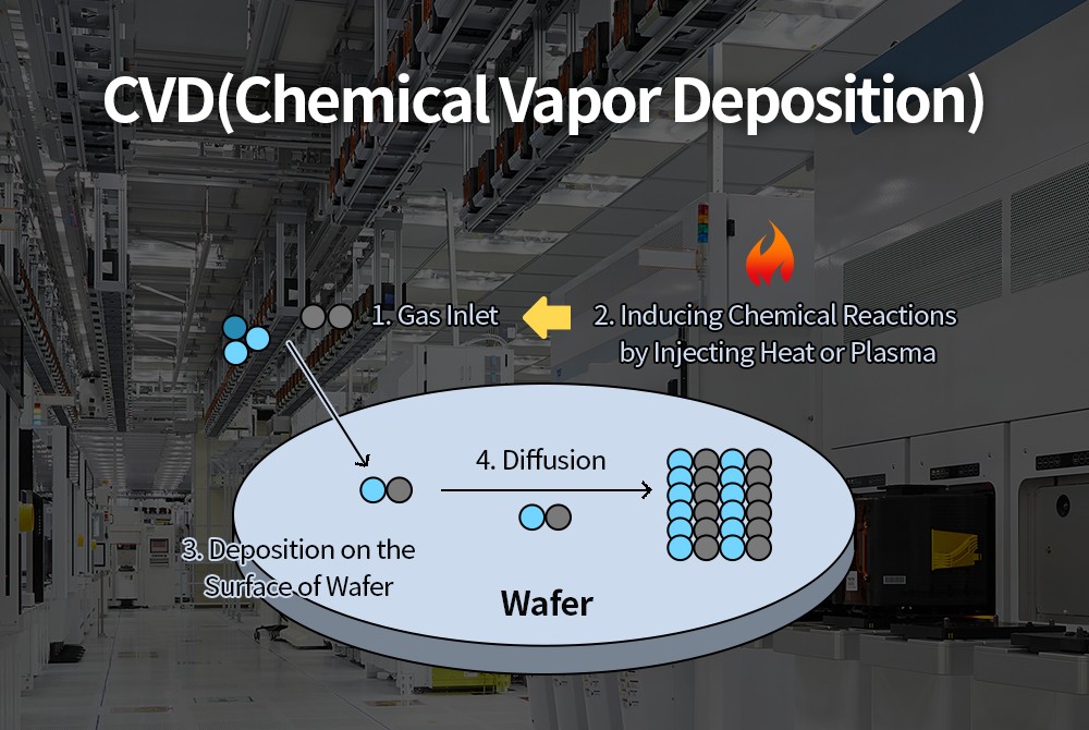
Chemical vapor deposition (CVD) is a process that utilizes gaseous substances to undergo chemical reactions on a substrate surface, generating a solid deposit that is then deposited onto the substrate as a film.
Simply put, vapors of gaseous or liquid reactants containing the elements that form the thin film, along with other gases required for the reaction, are introduced into a reaction chamber. Under certain conditions, these gaseous substances react chemically on the substrate surface, forming solid products that gradually deposit, ultimately forming a thin film. This film can be a metal, ceramic, semiconductor, or compound, and its composition and properties depend on the gaseous reactants used and the deposition conditions. The core of CVD technology lies in precisely controlling the chemical reactions of gaseous substances to achieve precise control of film growth, thereby achieving thin film materials with specific properties and quality requirements. Compared to other thin film deposition technologies, CVD offers unique advantages: it can produce high-purity, high-quality films with controllable composition and structure, and can achieve uniform deposition on complex substrate surfaces.
Principles of Chemical Vapor Deposition
CVD involves various types of chemical reactions, the most common of which include thermal decomposition, chemical synthesis, and chemical transport reactions.
- Thermal decomposition: Exploits the instability of a compound at high temperatures to decompose it into the desired element or compound, which is then deposited on the substrate surface. For example, silane (SiH₄) undergoes a thermal decomposition reaction at high temperatures (typically 800-1000°C): SiH₄(g) → Si(s) + 2H₂(g). Silicon atoms are deposited on the substrate to form a silicon film, while hydrogen is emitted as a byproduct. Many organometallic compounds can also be used to deposit metal films through thermal decomposition. For example, nickel carbonyl (Ni(CO)₄) decomposes upon heating into nickel and carbon monoxide: Ni(CO)₄(g) → Ni(s) + 4CO(g).
- Chemical synthesis: The target product is generated and deposited through a chemical reaction between different gaseous reactants. When depositing silicon dioxide films, silane and oxygen are used as reactants: SiH₄(g) + O₂(g) → SiO₂(s) + 2H₂(g). When forming silicon nitride films, silane and ammonia can be reacted at high temperatures: 3SiH₄(g) + 4NH₃(g) → Si₃N₄(s) + 12H₂(g).
- Chemical transport reactions are commonly used for purifying substances and growing single crystals. Taking the transport of zinc (Zn) by zinc iodide (ZnI₂) as an example, in the high-temperature region, Zn reacts with I₂ to form ZnI₂ vapor. The ZnI₂ vapor diffuses to the low-temperature region and decomposes, redepositing Zn, achieving Zn purification and directional growth: Zn(s) + I₂(g) ⇌ ZnI₂(g) (the reaction proceeds to the right in the high-temperature region, and to the left in the low-temperature region).
Deposition
CVD deposition is a complex physicochemical process consisting of the following steps:
Precursor delivery
The gaseous precursor (i.e., the gaseous compound involved in the reaction) is delivered into the reaction chamber via a carrier gas (e.g., inert gases such as nitrogen (N₂) and argon (Ar). The carrier gas carries the precursor and ensures its uniform distribution within the reaction chamber. The precursor delivery rate and concentration have a significant impact on deposition and film quality.
Adsorption
Adsorption: After the precursor gas molecules diffuse onto the substrate surface, they are adsorbed by the substrate. Physical adsorption is based on intermolecular van der Waals forces and is weak and reversible; chemical adsorption is based on chemical bonds to the substrate surface atoms and is stronger and relatively stable.
Reaction
Precursor molecules adsorbed on the substrate surface undergo a chemical reaction under the influence of energy such as heat, plasma, or laser light, producing solid products and volatile byproducts. Surface reactions are a key step in CVD, and their reaction rate and selectivity determine the film growth rate, composition, and structure. Different chemical reaction conditions (such as temperature, pressure, and energy input) lead to different reaction pathways and products.
Nucleation and Growth
Solid products generated by surface reactions form nuclei on the substrate surface. When the nuclei reach a certain critical size, they begin to grow. Nucleation and growth are influenced by various factors, such as temperature, supersaturation, and surface energy. As the reaction proceeds, the nuclei continue to grow and fuse together, ultimately forming a continuous film. Thin film growth can occur layer by layer (such as atomic layer deposition) or as islands that gradually merge to form a film.
Byproduct Removal
Volatile byproducts (such as gases) generated by surface reactions must be promptly removed from the reaction chamber to ensure smooth reaction progress and film quality. Byproducts are typically removed from the reaction chamber using a vacuum system. If byproducts are not effectively removed, they may re-adsorb onto the substrate surface, affecting the purity and performance of the film.
Types of Chemical Vapor Deposition
APCVD is chemical vapor deposition performed at atmospheric pressure. Its principle is to chemically react gaseous precursors and reactant gases at atmospheric pressure to form a film. APCVD’s key features are simple equipment, low cost, and high deposition rates, enabling large-area thin film deposition. However, since the reaction occurs at atmospheric pressure, the frequency of gas molecule collisions is high, potentially introducing a high number of impurities into the film.
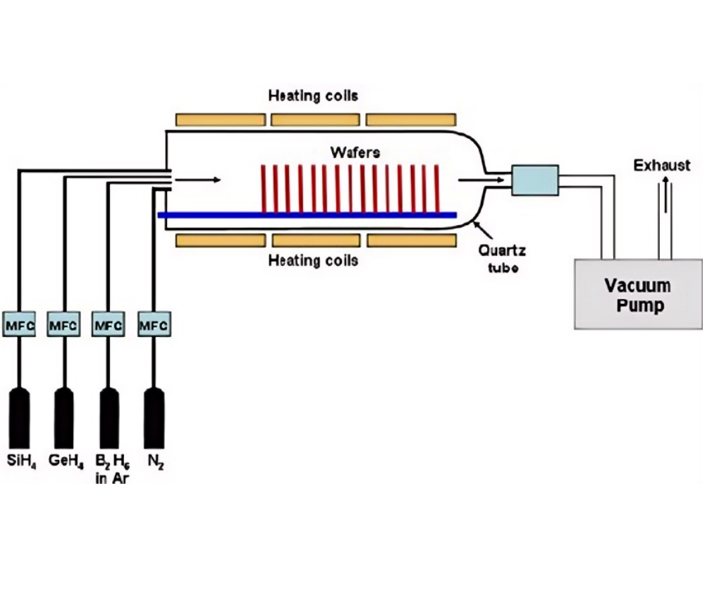
LPCVD is chemical vapor deposition performed at low pressure (typically 10⁻³ – 10⁻³ Torr). Low pressure increases the mean free path of gas molecules, reduces reactions in the gas phase, and predominates over surface reactions, resulting in more uniform film growth and higher quality. However, the equipment cost is relatively high, and the deposition rate is relatively slow. It is used in semiconductors to deposit thin films such as polysilicon, silicon nitride, and silicon dioxide.
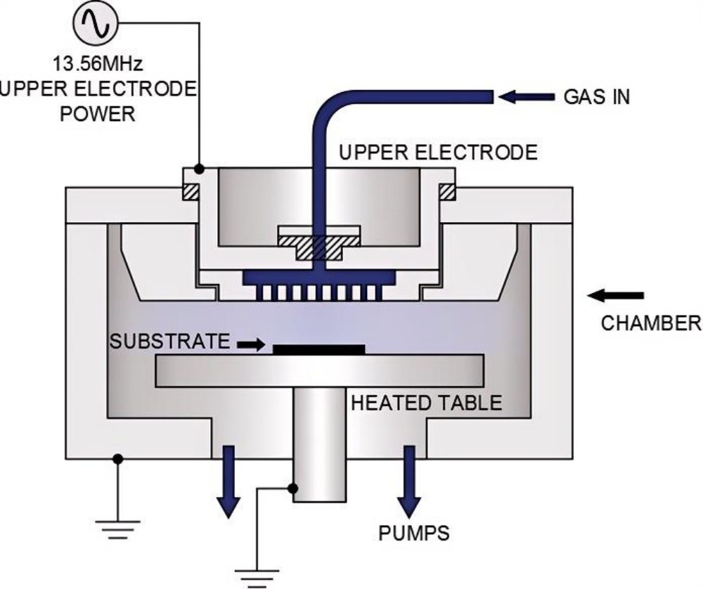
PECVD utilizes a low-temperature plasma generated by a gas glow discharge to enhance the chemical activity of reactants. Radio frequency (RF) or microwave (MW) power is applied to the reaction chamber to ionize the reactant gases, generating a plasma. High-energy electrons in the plasma collide with gas molecules, causing them to excite, dissociate, and ionize, significantly increasing reaction activity and lowering the required reaction temperature.
Technical Parameters
Temperature
Temperature is one of the key factors affecting the CVD reaction rate. According to Arrhenius's law, the reaction rate is exponentially related to temperature. As temperature increases, the thermal motion of molecules intensifies, and the reactant molecules gain more energy, significantly increasing the reaction rate.
Pressure
Pressure affects the equilibrium of chemical reactions. For some gas-phase reactions, changing the pressure can shift the reaction toward producing more products. Appropriately increasing the pressure can increase the concentration of reactants, promoting the reaction to the right, thereby improving the deposition rate and quality of the film.
Gas Flow Rate
The flow rates of precursor and carrier gases directly affect the deposition rate. Increasing the precursor gas flow rate increases the number of reactant molecules reaching the substrate surface per unit time, correspondingly increasing the deposition rate. The carrier gas flow rate primarily affects gas delivery and mixing. An appropriate carrier gas flow rate ensures uniform distribution of the precursor within the reaction chamber, improving deposition uniformity.
Reaction Time
Reaction time is a key factor in determining film thickness. Longer reaction times result in more material deposited on the substrate surface and a thicker film. By precisely controlling the reaction time, films of varying thickness requirements can be produced. Excessive reaction time may lead to the accumulation of defects in the film. For films with specific structures or properties, the reaction time should be rationally designed to optimize the film properties.
Chemical Vapor Deposition Substrates Materials
Metals
Many metals can serve as substrates for CVD, such as stainless steel, titanium alloys, aluminum alloys, and nickel-based alloys. Stainless steel, due to its excellent corrosion resistance and mechanical properties, is often used for depositing corrosion-resistant coatings on chemical equipment surfaces. Titanium alloys, with their high specific strength, excellent corrosion resistance, and biocompatibility, are used as substrates in the aerospace and biomedical fields, where ceramic coatings are deposited to further enhance their surface properties. Aluminum alloys are widely used in electronic device housings and automotive parts, and functional films such as wear-resistant and insulating films can be deposited via CVD.
Ceramics
Ceramic materials offer excellent properties such as high hardness, high-temperature resistance, and corrosion resistance. Common ceramic substrates include alumina, silicon nitride, and silicon carbide. Alumina ceramics offer excellent insulation and chemical stability and are commonly used as insulating substrates for electronic devices. Silicon nitride ceramics, with their high hardness, high strength, and excellent thermal stability, are widely used in high-temperature structural components and cutting tools. Silicon carbide ceramics, with their high thermal conductivity, high hardness, and wear resistance, are often used for components exposed to high temperatures, high pressures, and highly corrosive environments.
Semiconductors
Silicon is the most commonly used semiconductor material and dominates integrated circuit manufacturing. CVD plays a key role in silicon-based semiconductor manufacturing, depositing polysilicon for transistor gates, silicon dioxide for insulating layers, and silicon nitride for passivation layers. In addition to silicon, there are many compound semiconductor materials, such as gallium arsenide (GaAs), gallium nitride (GaN), and silicon carbide (SiC). These compound semiconductors possess unique electrical and optical properties, finding important applications in optoelectronics and high-frequency electronics.
Chemical Vapor Deposition Thin Film Materials
CVD technology has a wide range of applications and can be used to deposit thin films of various materials, including metals, semiconductors, and ceramics. The following are some typical materials that can be deposited using CVD.
Nonoxide ceramics
- Tantalum carbide (TaC)
- Tantalum nitride (TaN)
- Tantalum diboride (TaB2)
- Tungsten carbide (WC)
- Tungsten diboride (WB2)
- Hafnium carbide (HfC)
- Hafnium nitride (HfN)
- Hafnium diboride (HfB2)
- Zirconium carbide (ZrC)
- Zirconium nitride (ZrN)
- Zirconium diboride (ZrB2)
- Silicon carbide (SiC)
- Silicon nitride (Si3Ni4)
- Niobium carbide (NbC)
- Niobium nitride (NbN)
- Niobium diboride (NbB2)
- Titanium carbide (TiC)
- Titanium nitride (TiN)
- Titanium diboride (TiB2)
- Vanadium carbide (VC)
- Vanadium nitride (VN)
- Boron carbide (B4C)
- Boron nitride (BN)
Metals
- Rhenium (Re)
- Tantalum (Ta)
- Tungsten (W)
- Niobium (Nb)
- Molybdenum (Mo)
- Iridium (Ir)
- Platinum (Pt)
- Boron (B)
- Silicon (Si)
- Metal alloys: W-Re, Ta-W,
- Mo-Re, Ir-Pt
Oxide ceramics
- Alumina (Al2O3)
- Hafnia (HfO2)
- Silica (SiO2)
- Tantala (Ta2O5)
- Titania (TiO2)
- Yttria (Y2O3)
- Zirconia (ZrO2)
Advantages of Chemical Vapor Deposition
High Film Quality
Precisely controlling the reaction effectively minimizes impurity introduction, resulting in the production of high-purity thin films. The resulting films exhibit a dense structure and excellent adhesion, which is crucial for the performance of microelectronic devices.
Precise Control of Composition and Structure
Finely adjusting parameters such as the type, flow rate, and ratio of the reactant gases, as well as reaction temperature and pressure, allows for precise control of the chemical composition and microstructure of the film, enabling precise regulation of film properties.
Uniform Deposition over Large Areas
CVD technology can achieve highly uniform thin film deposition on large substrates. The uniform deposition characteristics of CVD technology are crucial for ensuring consistent film properties across the entire substrate.
Various Materials Deposition Options
It can deposit thin films of a wide variety of materials, including metals, ceramics, semiconductors, and compounds. It can also produce various composite thin films, meeting the diverse material performance requirements of various applications.
Suitable for Complex Substrates
Because gaseous substances react and deposit on the substrate surface, CVD technology is not restricted by substrate shape and can achieve uniform thin film deposition on substrates with complex three-dimensional shapes. For some parts with complex structures such as deep holes and grooves, CVD technology can also deposit high-quality films inside these structures.
Disadvantages of Chemical Vapor Deposition
High Equipment Cost
CVD equipment is typically complex, requiring precise gas delivery systems, vacuum systems (for low-pressure CVD and PECVD), heating systems, and reaction monitoring systems, all of which contribute to high equipment costs.
High Operating Costs
CVD consumes large quantities of gaseous reactants and carrier gases. These gases are often expensive and require regular replacement. The operation of the vacuum system also consumes significant energy.
Reaction Temperature Limitations
Although some CVD techniques (such as PECVD) can deposit at relatively low temperatures, high temperatures may affect the properties of the substrate material in some cases where high-quality thin films are required. This can limit their application on temperature-sensitive substrates.
Reaction Byproduct Handling
CVD produces some gaseous byproducts. These byproducts can be corrosive, toxic, or flammable and explosive, requiring proper handling. Handling these byproducts requires additional equipment and costs, increasing the complexity and cost of the overall process.
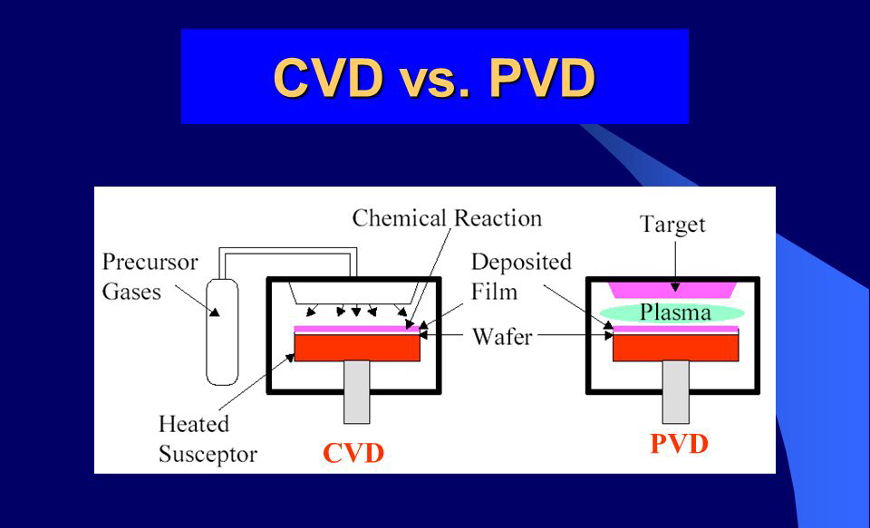
Chemical Vapor Deposition vs. Physical Vapor Deposition
Physical vapor deposition (PVD) is also a commonly used thin film deposition technique. It uses physical methods (such as evaporation and sputtering) to vaporize a material into atoms or molecules, which are then deposited on a substrate to form a thin film. CVD and PVD differ in their principles, process characteristics, and applications.
Principle Difference
CVD is based on a chemical reaction, utilizing gaseous reactants to react on the substrate surface to form a solid deposit, which then forms a film. PVD, on the other hand, uses physical methods (such as heated evaporation and ion sputtering) to directly convert the material from a solid to a gaseous state, which is then condensed and deposited on the substrate surface to form a film. For example, in CVD, silicon dioxide thin films are deposited by a chemical reaction between silane and oxygen. In PVD, sputtering involves bombarding a target with high-energy ions, sputtering target atoms and depositing them on the substrate.
Process Characteristics Comparison
Temperature: CVD typically operates at higher temperatures (some CVD variants, such as PECVD, can deposit at lower temperatures). High temperatures facilitate certain chemical reactions and improve film crystal quality, but may also thermally impact the substrate. PVD generally operates at relatively low temperatures (e.g., 300-500°C), effectively avoiding thermal damage to already formed fine structures and heat-sensitive materials on the wafer. In semiconductor manufacturing, when thin films need to be deposited on partially processed wafers, PVD’s low temperature advantage ensures that previously formed transistors, circuits, and other structures are not affected by high temperatures.
Film Quality: CVD-produced films exhibit high purity, excellent crystal quality, strong substrate adhesion, and excellent step coverage, enabling uniform deposition on complex substrate surfaces. PVD-produced films typically have higher density and purity, and offer high-precision film thickness control, enabling atomic-level control. However, step coverage on complex substrates is relatively poor.
Deposition Rate: PVD has a relatively fast deposition rate, enabling thin film deposition in a shorter time, improving production efficiency. While CVD’s deposition rate can be relatively slow in some cases, it can still meet certain production requirements through process optimization.
Application Focus: CVD, due to its ability to precisely control film composition and structure, as well as its excellent step coverage, is crucial in semiconductor manufacturing for the deposition of various functional thin films (such as transistor gates, insulating layers, and passivation layers), as well as dielectric and metal layers in multi-layer wiring of integrated circuits. PVD is widely used in applications requiring low-temperature deposition, extremely precise film thickness control, and high surface flatness, such as in the manufacture of hard drive heads, optical lens coating, and the preparation of decorative coatings.
Applications of Chemical Vapor Deposition
In the semiconductor and integrated circuit fields, CVD technology is one of the core processes for achieving high-performance chip manufacturing. In the solar cell field, it helps improve photoelectric conversion efficiency and promote the development of renewable energy. It also plays an indispensable role in fields such as optics, aerospace, mechanics, nanomaterials, and biomedicine.
Semiconductors
In transistor manufacturing, CVD technology is used to deposit polysilicon as the gate material. By precisely controlling the growth and doping of polysilicon, transistor performance can be optimized, increasing electron mobility and switching speed. Depositing insulating materials such as silicon dioxide and silicon nitride as gate oxide and passivation layers protects the transistor from environmental influences, improving device stability and reliability.
Solar Cells
In crystalline silicon solar cells, CVD technology is used to deposit antireflection coatings, such as silicon nitride thin films, which reduce light reflection and improve the cell’s light absorption efficiency, thereby enhancing photoelectric conversion efficiency. For some compound solar cells, such as gallium arsenide (GaAs) and copper indium gallium selenide (CIGS), CVD technology can be used to grow high-quality semiconductor epitaxial layers, precisely controlling the material composition and structure, thereby improving cell performance and stability. In GaAs solar cells, metal-organic chemical vapor deposition (MOCVD) can be used to grow high-quality GaAs epitaxial layers, achieving efficient photoelectric conversion.

Optics
Depositing antireflective coatings on the surfaces of optical lenses and components is one of the key applications of CVD technology. By depositing thin films with a specific refractive index and thickness (such as silicon dioxide and titanium oxide), light reflection at interfaces can be reduced, improving the transmittance of optical components. These films are widely used in applications such as camera lenses, telescopes, and eyeglass lenses. In optical thin-film devices such as distributed Bragg reflectors (DBRs) and Fabry-Perot interferometers, CVD technology precisely controls the thickness and refractive index of multilayer thin films, enabling precise manipulation of light. These applications are widely used in laser technology, optical communications, optical sensors, and other fields.
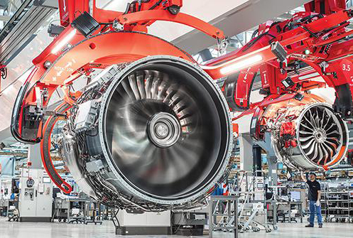
Aerospace
CVD technology is used to deposit ceramic coatings (such as silicon carbide and silicon nitride) on the surfaces of high-temperature components such as aerospace engines and gas turbines. These coatings offer high-temperature resistance, oxidation resistance, and wear resistance, effectively protecting high-temperature components and improving their service life and reliability. Silicon carbide coatings deposited on aircraft engine blades can enhance their oxidation resistance and wear resistance in high-temperature gas environments.
Conclusion
Chemical vapor deposition (CVD) is an important thin film deposition technique. It generates solid deposits through chemical reactions between gaseous chemicals on the substrate surface. It offers advantages such as excellent deposition uniformity, precise control of film composition and thickness, and suitability for complex substrate shapes. CVD primarily involves steps such as precursor selection, chamber preparation, gas delivery and control, reaction, film growth, and post-processing. Each step significantly impacts the quality and performance of the film.
Depending on the process conditions, CVD can be categorized into various types, including atmospheric pressure chemical vapor deposition (APCVD), low-pressure chemical vapor deposition (LPCVD), plasma-enhanced chemical vapor deposition (PECVD), and metal-organic chemical vapor deposition (MOCVD). Each type has its own unique principles, characteristics, and application scenarios. Optimizing technical parameters such as temperature, pressure, gas flow and ratio, and reaction time is key to achieving high-quality thin films.