The Ultimate Guide to DC Magnetron Sputtering
DC sputtering is applicable to a variety of metals, alloys and some conductive compounds, and can produce thin films with different functions to meet the diverse needs of various industries for thin film performance. However, this technology also has certain limitations.
- Low Cost
- Good Film Uniformity
- Higher Film Deposition Rate
- Strong Film-Substrate Bonding
- Compatible With Conductive Materials
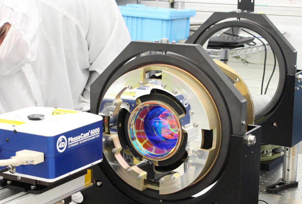
Wstitanium Workshop
Our Powerful Facilities
Everything You Should Know About DC Sputtering
In the field of material surface treatment and film preparation, DC sputtering, as an important physical vapor deposition (PVD) technology, plays a key role. From the demand for ultra-fine conductive films in semiconductor chip manufacturing, to the pursuit of high-purity optical films in optical devices, to the application of surface strengthening coatings for mechanical parts, DC sputtering technology has become an indispensable technology in many industries due to its unique advantages. This blog will comprehensively and in-depth introduce DC sputtering, including its principles, working process, commonly used materials, advantages and disadvantages, comparison with other sputtering technologies, and a wide range of applications, aiming to provide you with a comprehensive understanding and practical guidance on DC sputtering.
What is DC sputtering?
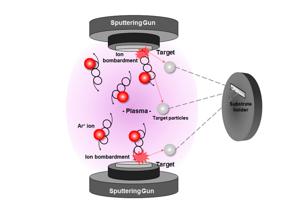
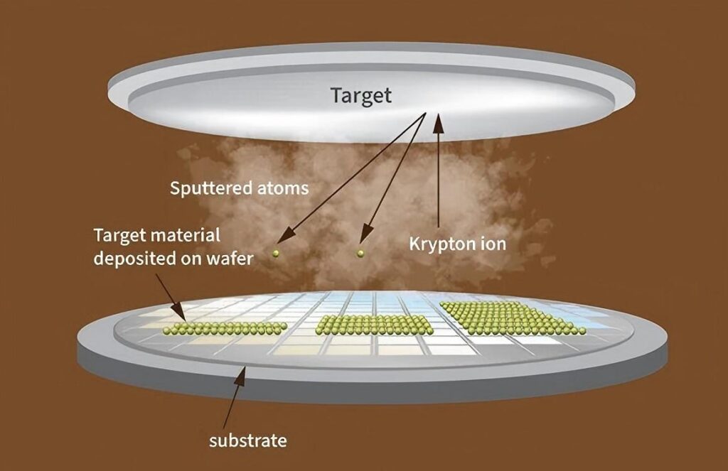
DC sputtering is a type of physical vapor deposition (PVD) technology, which refers to the technology of sputtering and coating by bombarding the target material with ions generated by DC glow discharge. In a typical DC sputtering system, it is mainly composed of a vacuum chamber, a vacuum system and a DC sputtering power supply. The vacuum chamber provides a low-pressure environment for the entire sputtering process, reduces the scattering of sputtered particles by gas molecules, and ensures that the sputtered atoms can smoothly reach the substrate surface. The vacuum system is responsible for pumping the vacuum chamber to a high vacuum state, which usually needs to reach 10⁻³ – 10⁻⁵ Pa. The DC sputtering power supply applies a DC voltage between the two electrodes (cathode and anode) in the vacuum chamber, and the voltage generally ranges from 2 to 3 kV.
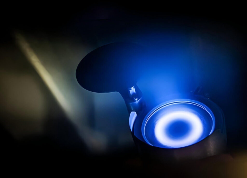
The target is installed on the cathode surface, and the substrate or workpiece is placed on the sample stage as the anode. When the vacuum chamber reaches the predetermined vacuum degree, an inert gas such as argon is introduced and the gas pressure is maintained at about 1.0 Pa. At this time, applying a DC voltage between the two electrodes will produce a glow discharge phenomenon. A high-density plasma zone, i.e., the negative glow zone, is formed near the target (cathode). Argon ions in the negative glow zone bombard the target surface at high speed under the acceleration of DC voltage. Since the ions have high energy, when they collide with target atoms, they can knock target atoms out of the surface, which is the sputtering effect. The sputtered target atoms fly freely in the vacuum and eventually deposit on the surface of the substrate or workpiece, gradually forming a thin film.
The first step of DC sputtering is to create a plasma in a vacuum environment. When a high DC voltage is applied between the two electrodes of the vacuum chamber, the argon molecules that were originally in a neutral state begin to ionize. Under the action of the strong electric field, electrons are pulled out from the surface of the cathode (target material) and accelerated in the electric field. These high-speed electrons collide with argon molecules, knocking out the electrons in the argon molecules, turning the argon molecules into positively charged argon ions and free electrons, thus forming a plasma. This process can be simply represented by the following reaction formula: Ar (neutral argon molecules) + e⁻ (electrons) → Ar⁺ (argon ions) + 2e⁻. As more electrons collide with argon molecules, the concentration of ions and electrons in the plasma continues to increase, forming a stable plasma area, mainly concentrated in the negative glow area near the target (cathode).
Ion Bombardment Target
The argon ions formed in the negative glow area are positively charged and are accelerated by the DC electric field to move at high speed toward the cathode (target) surface. When argon ions hit the target surface, the kinetic energy they carry is transferred to the target atoms. If the energy of the argon ions is high enough, they can overcome the binding force between the target atoms and knock the target atoms out of the surface. This process is called sputtering. The sputtered target atoms have a certain energy and speed, and are ejected from the target surface in the form of atoms or atomic clusters into the vacuum space. In sputtering, the sputtering yield of target atoms (that is, the number of atoms sputtered from the target surface by each incident ion) is related to many factors, including the energy of the ion, the angle of incidence, the atomic mass of the target, the crystal structure, and the binding energy. Generally speaking, the higher the ion energy, the greater the sputtering yield; when the ions are incident at a certain angle, the sputtering yield will reach a maximum at a certain angle.
Deposition
The atoms sputtered from the target surface perform irregular thermal motion in a vacuum, and some of them fly to the substrate surface. When these atoms reach the substrate surface, due to the relatively low substrate temperature, the kinetic energy of the atoms decreases rapidly and they are adsorbed by the substrate surface. As more and more target atoms are deposited on the substrate surface, the atoms begin to interact with each other and gradually form atomic clusters. These clusters continue to absorb the surrounding atoms, gradually increase in size, and eventually connect to form a continuous film. During the film growth process, factors such as the atomic deposition rate, substrate temperature, and substrate surface state will affect the quality and structure of the film. For example, a higher deposition rate may lead to a loose film structure, while appropriately increasing the substrate temperature can promote the diffusion of atoms on the substrate surface, making the film denser and more uniform.
Advantages of DC Sputtering
DC sputtering technology, as a mature physical vapor deposition method, has shown many significant advantages in the field of thin film preparation, making it widely used in industry and scientific research:
Low Cost
The DC sputtering system is mainly composed of basic components such as vacuum chamber, DC power supply, vacuum system, etc. Compared with other complex thin film preparation technologies (such as molecular beam epitaxy, chemical vapor deposition, etc.), its equipment structure is simpler and the manufacturing and maintenance costs are lower.
High deposition rate
In DC sputtering, a higher film deposition rate can be achieved by adjusting parameters such as the power of the DC power supply and the working gas pressure. A higher deposition rate can shorten the production cycle and improve production efficiency, and is especially suitable for large-scale industrial production to meet the needs of mass production.
Good film uniformity
Reasonably design the target shape, the relative position of the substrate and the target, and optimize the sputtering parameters. DC sputtering can produce thin films with good uniformity. The uniformity of thin films is crucial for many applications, such as optical films require good thickness uniformity to ensure the consistency of optical properties, and conductive films in electronic devices require uniform thickness and electrical properties to ensure the stability of the device.
Strong bonding force
High-energy ions bombard the target material, so that the sputtered atoms have a certain energy. When these atoms are deposited on the substrate surface, they can interact strongly with the substrate surface to form chemical bonds or diffusion bonds, so that the film and the substrate have a strong bonding force. Strong bonding force can ensure that the film is not easy to fall off during use, and improve the life and reliability of the film.
Compatible with conductive materials
DC sputtering technology can deposit a variety of metals, alloys and some conductive compound materials, and has a wide range of applications. Whether it is a high-melting point metal (such as tungsten, molybdenum) or a low-melting point metal (such as tin, zinc), high-quality thin films can be prepared by DC sputtering to meet the needs of different fields for different material films.
Parameters are easy to control
The main parameters of DC sputtering, such as sputtering power, working gas pressure, distance between target and substrate, substrate temperature, etc., can be precisely controlled by corresponding equipment. By optimizing these parameters, the thickness, composition, structure and performance of the film can be precisely controlled, so as to prepare a film that meets specific needs.
Disadvantages of DC sputtering
Although DC sputtering technology has many advantages, it also has some inherent disadvantages that need to be considered and resolved in practical applications:
Applicable only to conductive targets
DC sputtering relies on the conductivity of the target to maintain glow discharge. When using insulating materials as targets, positive ions will accumulate on the surface of the target to form a space charge layer, which will increase the surface potential of the target and eventually extinguish the glow discharge, making it impossible to perform effective sputtering. Therefore, DC sputtering technology is only applicable to the sputtering of conductive materials such as metals and alloys, but not to insulating materials such as ceramics and oxides, which limits its scope of application.
Target poisoning is easy to occur
When reactive gases (such as oxygen, nitrogen, etc.) are introduced into sputtering to prepare compound films, the reactive gases may react chemically with the surface of the target to form a compound layer. These compounds are usually insulating or semiconductor materials, which will increase the surface resistance of the target, affect the stability of the glow discharge, and even cause the target to be “poisoned”. Target poisoning will reduce the sputtering rate, make the film composition difficult to control, and seriously affect the quality and performance of the film.
Internal stress in the film
In DC sputtering, after high-energy particles bombard the target material, the sputtered atoms are deposited on the substrate surface with a certain amount of energy. These atoms may produce lattice distortion and defects during deposition, resulting in internal stress inside the film. Excessive internal stress can cause cracking and shedding of the film, reducing the service life and performance stability of the film.
Narrow gas pressure range
DC sputtering requires a specific working gas pressure range (usually 0.1-10 Pa) to stably perform glow discharge. If the gas pressure is too low, the number of ions is insufficient, and it is difficult to maintain a stable plasma; if the gas pressure is too high, the probability of collision between ions and gas molecules increases, which will reduce the energy of the ions and affect the sputtering effect and film quality.
The substrate temperature is easy to rise
In sputtering, when high-energy ions and sputtered atoms bombard the substrate surface, they will transfer part of the energy to the substrate, causing the substrate temperature to rise. For some temperature-sensitive substrate materials (such as plastics, polymers, etc.), excessively high temperatures may cause deformation, performance degradation, or even damage to the substrate, limiting the application of DC sputtering technology on the surface of these materials.
Complex-shaped substrates are a challenge
For substrates with complex shapes (such as grooves, holes, curved surfaces, etc.), DC sputtering technology is difficult to ensure the uniformity of the film in all parts of the substrate. Due to the strong directionality of sputtered atoms, the film thickness is thin or cannot be deposited in the shadow area of the substrate, affecting the overall performance of the film.
DC Sputtering vs. RF Sputtering
RF sputtering (radio frequency sputtering) is a technology that uses a high-frequency alternating electric field generated by an RF power supply to achieve sputtering coating. Unlike DC sputtering, the power supply output frequency of RF sputtering is usually a 13.56 MHz RF signal. In an RF sputtering system, the target material can be a conductive material or an insulating material. When the RF power supply is applied to the target material, due to the action of the high-frequency alternating electric field, the electrons can obtain enough energy in the electric field, continuously collide with gas molecules to ionize them, and form a stable plasma. In the positive half cycle of the alternating electric field, positive ions will move toward the target material (equivalent to the cathode at this time) and bombard the target material. In the negative half cycle, electrons move toward the target material, neutralize the accumulation of positive charges on the surface of the target material (especially important for insulating targets), thereby avoiding the accumulation of charges on the surface of the target material and ensuring the stability of the sputtering process.
| Comparison Item | DC Sputtering | RF Sputtering (Radio Frequency Sputtering) |
| Definition | A technology that utilizes DC glow discharge to generate ions to bombard the target material for sputtering coating. | A technology that uses a 13.56MHz radio frequency alternating electric field to generate glow discharge to achieve sputtering coating. |
| Cost | The equipment structure is simple, mainly using DC power supply, with low manufacturing and maintenance costs, and low initial investment and operating costs. | It requires the use of radio frequency power supply and impedance matching network and other auxiliary equipment, the manufacturing process is complex, and the cost is high. The initial investment and maintenance costs are higher than those of DC sputtering. |
| Principle | Based on DC glow discharge, the DC electric field accelerates positive ions to bombard the cathode (target material), and the discharge is maintained depending on the conductivity of the target material. | Using radio frequency alternating electric field, electrons gain energy to ionize gas to form plasma. The alternating characteristics can neutralize the positive charges on the surface of insulating target materials and maintain stable sputtering. |
| Deposition Rate | For conductive target materials, the deposition rate is usually higher under the same power, the ion acceleration is direct, and the energy transfer efficiency is high. | For conductive target materials, the deposition rate is generally lower than that of DC sputtering, and the ion acceleration efficiency of radio frequency electric field is low; it is a feasible method for insulating target materials, and the rate depends on the properties of the target material and radio frequency power, etc. |
| Operating Pressure | Usually in the range of 1-10Pa, higher pressure is conducive to maintaining the stability of glow discharge. | It can work in the range of 0.1-1Pa. Lower pressure reduces the scattering of gas molecules on sputtered atoms and improves the density and purity of the thin film. |
| Material Compatibility | Only applicable to conductive materials (metals, alloys, etc.), insulating materials cannot maintain discharge due to charge accumulation. | It has wider compatibility and can sputter conductive materials, insulating materials (ceramics, oxides, etc.) and semiconductor materials. |
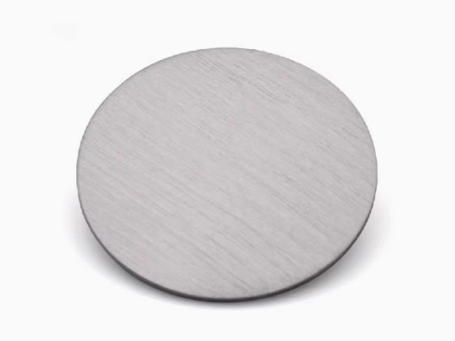
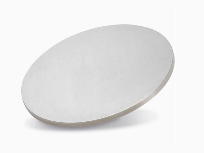
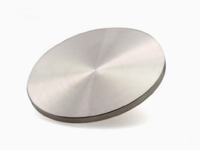
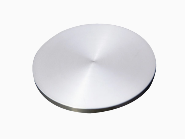
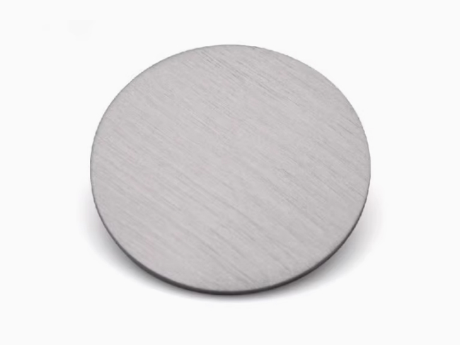
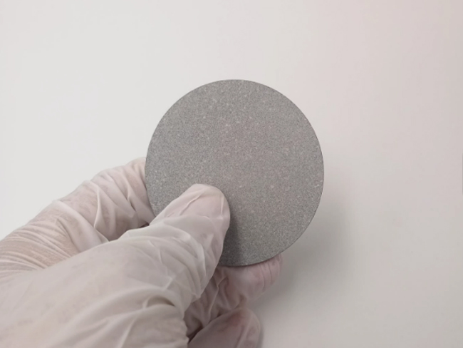
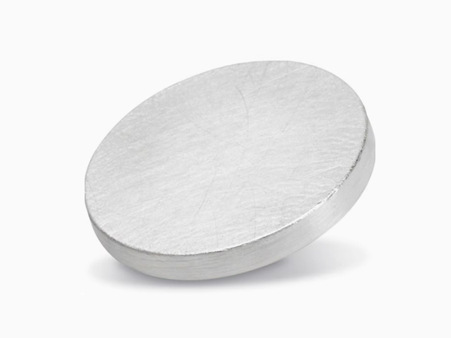
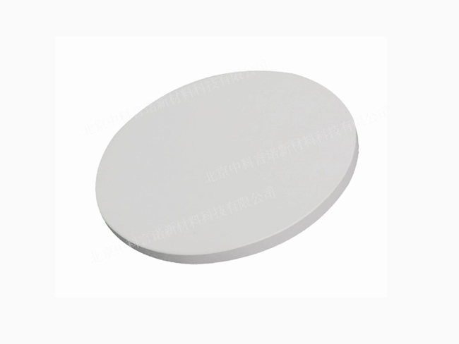
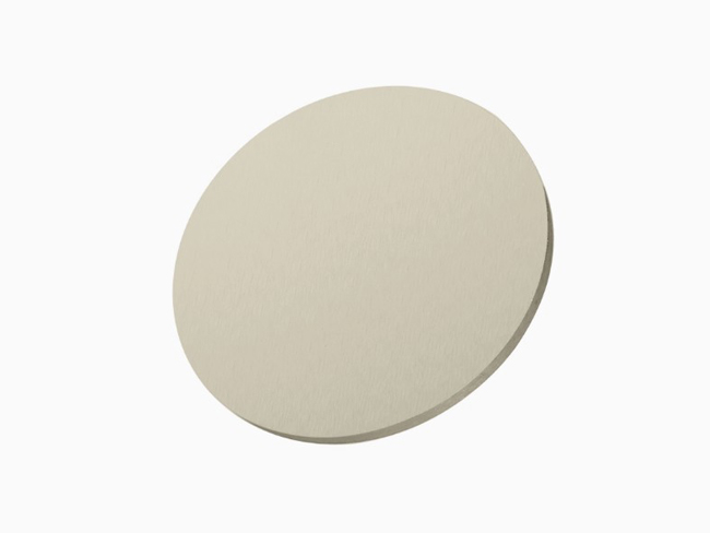
Material plays a core role in DC sputtering and is directly related to the performance, quality and application fields of the film. Different materials show different sputtering characteristics and deposition behaviors in DC sputtering due to their unique physical and chemical properties. As one of the most commonly used target materials in DC sputtering, metal materials have good electrical conductivity, high sputtering efficiency and diverse physical properties, and are widely used in electronics, optics, energy and other fields.
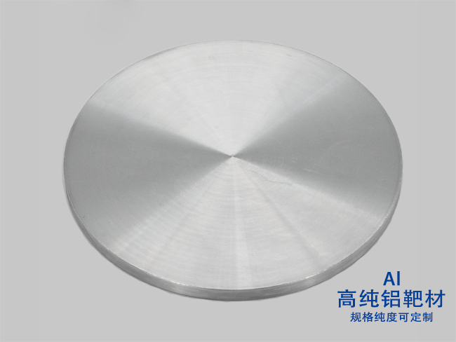
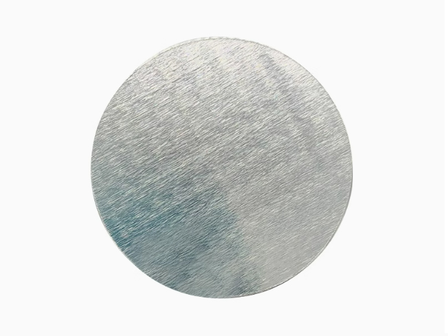
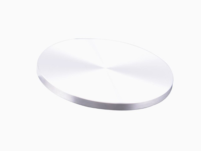
Aluminum (Al) Sputtering Target
Aluminum is a metal material widely used in DC sputtering. It has the characteristics of low density, good electrical conductivity, excellent thermal conductivity and relatively low cost. Its density is about 2.7 g/cm³. In the field of optics, aluminum film can be used as a reflector coating. In the packaging industry, aluminum film is used for food and drug packaging.
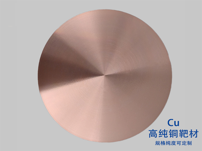
Copper (Cu) Sputtering Target
Copper has extremely high electrical and thermal conductivity, with an electrical conductivity of about 5.96×10⁷ S/m and a thermal conductivity of 401 W/(m・K). Copper is an ideal material for manufacturing ultra-large-scale integrated circuit interconnects and chip packaging. Copper film also effectively shields electromagnetic interference.
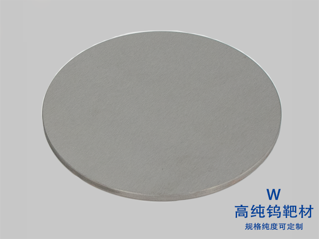
Tungsten (W) Sputtering Target
Tungsten has an extremely high melting point of 3422℃, high hardness, high density (19.3 g/cm³) and good high temperature strength. Tungsten is often used to manufacture gates and interconnects in integrated circuits. Tungsten alloy coatings are also used to manufacture high temperature resistant parts of aircraft.
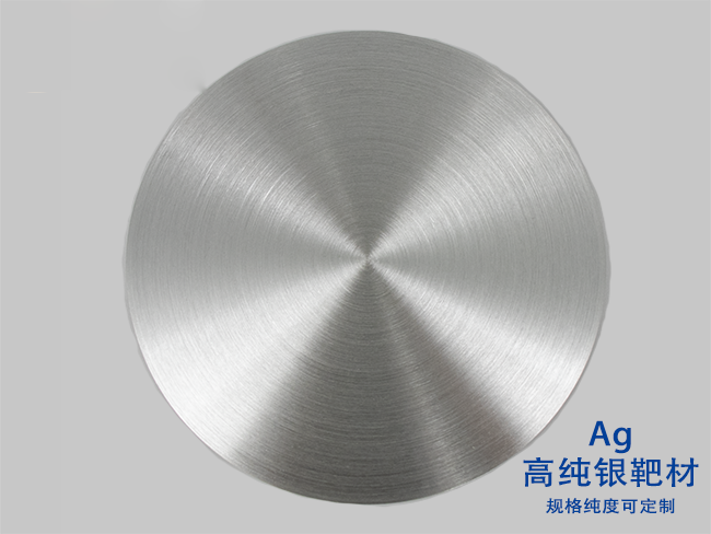
Silver (Ag) Sputtering Target
Silver has the highest electrical conductivity of all metals, about 6.3×10⁷ S/m. This makes it important in electronic circuits, especially in parts with extremely high conductivity requirements, such as high-frequency circuits, electrodes of superconducting devices, etc. Silver film is also a high-quality material for making reflectors.
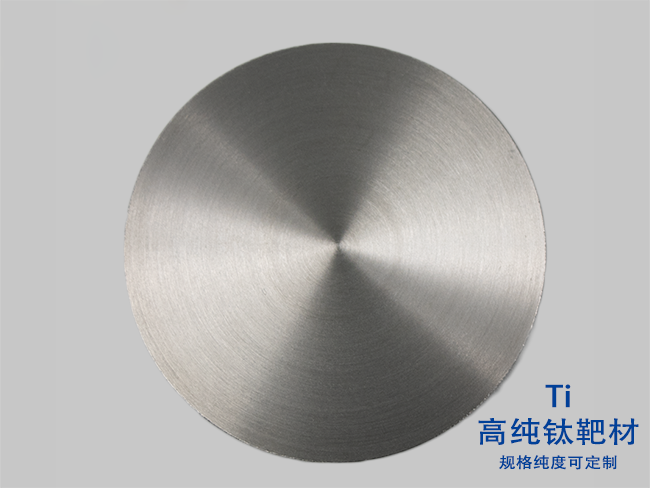
Titanium (Ti) Sputtering Target
Titanium has excellent properties such as low density (about 4.5 g/cm³), high strength, high temperature resistance, and corrosion resistance. Titanium has good biocompatibility and is widely used in artificial joints, dental implants, etc. Titanium-coated equipment is also used for corrosion-resistant reaction vessels and pipelines.
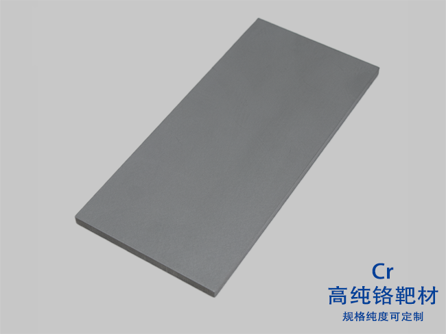
Chromium (Cr) Sputtering Target
Chromium has the characteristics of high hardness, good wear resistance, and strong corrosion resistance. Chrome plating is often used to improve the surface hardness and wear resistance of parts. Chromium also serves as an adhesion layer for metal interconnect layers to improve the bonding strength of different metal layers.
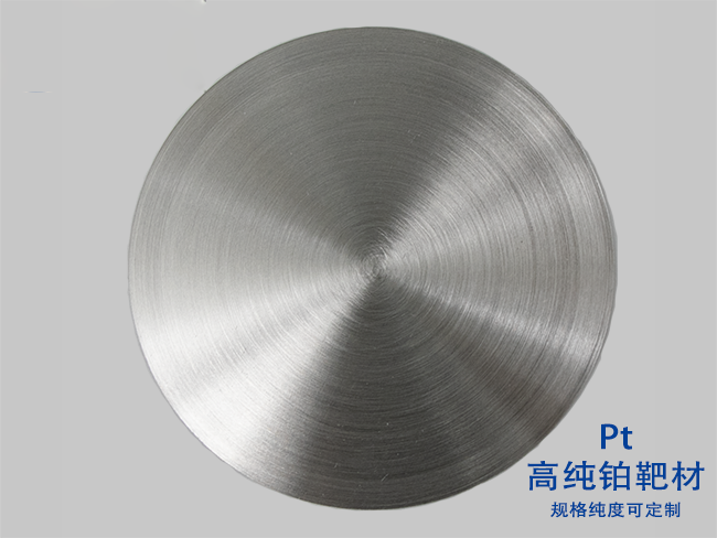
Platinum (Pt) Sputtering Target
Platinum has excellent chemical stability, catalytic activity and high temperature resistance. Platinum catalysts are widely used in petrochemicals, fine chemicals and other fields. Platinum, as an electrode catalyst, can accelerate the electrochemical reaction of hydrogen and oxygen.
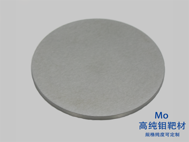
Molybdenum (Mo) Sputtering Target
Molybdenum has a high melting point (2623℃), good thermal stability and conductivity. It is often used to manufacture electrodes and leads for semiconductor devices. Molybdenum can also be added to steel as an alloying element to improve the strength, hardness and corrosion resistance of steel.
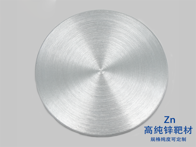
Zinc (Zn) Sputtering Target
Zinc has good corrosion resistance and a low melting point. The galvanized layer is one of the most widely used anti-corrosion coatings. Zinc is an important negative electrode material for zinc-manganese batteries, zinc-air batteries, etc., and its ability to lose electrons in chemical reactions is used to achieve the discharge function of the battery.
Nickel (Ni) Sputtering Target
Nickel has good corrosion resistance, high temperature stability and magnetism. Nickel coating can be used to prevent equipment from being corroded by chemical media. Nickel-iron alloy films are often used to manufacture magnetic storage media. Nickel-based alloy coatings can improve the high temperature resistance of parts.
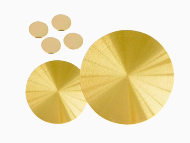
Gold (Au) Sputtering Target
Gold is a precious metal with stable chemical properties and good electrical conductivity. Gold plating is often used in key parts of electronic devices, such as chip pins and connectors. Gold film is also used to make high-reflectivity mirrors and optical filters, which have good reflection and transmission characteristics for light of specific wavelengths.
Cobalt (Co) Sputtering Target
Cobalt has good magnetic properties and high temperature strength. Cobalt-based alloy films are often used to make high-performance permanent magnetic materials, such as magnetic heads in hard disk drives, permanent magnets in motors, etc. Cobalt also improves the high temperature strength and oxidation resistance of the alloy.
Tantalum (Ta) Sputtering Target
Tantalum has excellent corrosion resistance, especially strong resistance to various acid, alkali and other chemical media. Tantalum-coated reactors, pipelines, etc. play an important role in the pharmaceutical, electronic chemical production and other industries. Tantalum capacitors effectively store and release charges to ensure the stable operation of circuits.
Niobium (Nb) Sputtering Target
Niobium has good superconductivity, corrosion resistance and high temperature strength. Niobium-titanium alloys and niobium-tin alloys are often used to manufacture superconducting magnets, which are used in large scientific devices such as nuclear magnetic resonance imaging (MRI) equipment and particle accelerators to generate strong magnetic fields.
Palladium (Pd) Sputtering Target
Palladium is a precious metal with good catalytic properties and chemical stability. In automobile exhaust purification catalysts, palladium promotes the redox reaction of harmful gases such as carbon monoxide, hydrocarbons and nitrogen oxides. Palladium can be used to manufacture electrodes for multilayer ceramic capacitors to improve the performance and reliability of capacitors.
Iron (Fe) Sputtering Target
Iron has high strength and magnetism. DC sputtering deposits various functional coatings on the surface of steel, such as corrosion-resistant zinc coatings, chromium coatings, etc., to improve the performance and life of steel. Iron-based soft magnetic material films can be used to manufacture transformer cores, inductors, etc. .
Tin (Sn) Sputtering Target
Tin has a low melting point (231.9℃), good solderability and corrosion resistance. Tin-based solder is the most commonly used welding material, such as tin-lead solder, lead-free solder (such as tin-silver-copper alloy solder), etc. In the food packaging industry, tin-plated steel sheets (tinplate) are widely used in the manufacture of food cans.
Rhodium (Rh) Sputtering Target
Rhodium is a rare and precious metal with high reflectivity, good chemical stability and catalytic properties. Rhodium film is often used to make mirrors with high reflectivity, such as in astronomical telescopes, laser reflectors, etc. Rhodium is also used to make electrodes and contacts for electronic devices.
Bismuth (Bi) Sputtering Target
Bismuth is a low melting point metal with a melting point of 271.4℃. Bismuth-based alloy films can be used to manufacture electronic components such as thermistors and varistors. Bismuth can be added to other metals as an additive to improve the properties of metals, such as improving the corrosion resistance and processing performance of lead.
Antimony (Sb) Sputtering Target
Antimony has a certain hardness and brittleness. Compound semiconductor materials such as indium antimonide (InSb) have good photoelectric properties and are often used to manufacture photoelectric devices such as infrared detectors and Hall elements. Antimony can be used as an alloying element to improve the hardness and strength of the alloy.
Cadmium (Cd) Sputtering Target
Cadmium has good corrosion resistance and a low melting point. Cadmium plating is often used for corrosion protection of steel parts, especially in marine environments or other harsh corrosive environments. However, due to the toxicity of cadmium, its use is subject to certain restrictions.
Ag-Pd Sputtering Target
Silver-palladium alloy combines the good conductivity of silver with the chemical stability and catalytic properties of palladium. It is often used to make electrical contact materials, such as relay contacts, electrodes of precision electronic components, etc., maintaining good conductivity and resistance to arc erosion.
Gallium (Ga) Sputtering Target
Gallium is a low-melting-point metal with a melting point of 29.76°C. Compound semiconductor materials such as gallium nitride (GaN) and gallium arsenide (GaAs) have excellent electrical properties. Gallium-based alloys can be used to make low-melting-point alloys for electronic packaging, fuses, etc.
Indium (In) Sputtering Target
Indium has a low melting point (156.6°C), good ductility and conductivity. Indium tin oxide (ITO) film is a transparent conductive film with high transparency and good conductivity. It is widely used in flat panel display devices such as liquid crystal displays (LCDs), organic light-emitting diode displays (OLEDs), and touch screens.
Tellurium (Te) Sputtering Target
Tellurium often forms compounds with other elements for various functional materials. The Seebeck effect of bismuth telluride is used to achieve the conversion of thermal energy to electrical energy. Bismuth telluride can also achieve the Peltier effect, that is, cooling at one end and heating at the other end.
Scandium (Sc) Sputtering Target
Sc is a rare earth metal with low density, high melting point and good chemical stability. Scandium aluminum alloy film meets the requirements of aircraft for high performance and lightweight materials. Scandium alloy coating can improve the strength and durability of sports equipment while maintaining good lightweight characteristics.
Yttrium (Y) Sputtering Target
Yttrium has important applications in the fields of high-temperature superconducting materials and ceramic materials. Yttrium barium copper oxide (YBCO) is a typical high-temperature superconducting material with a high superconducting transition temperature, which can achieve superconducting state above liquid nitrogen temperature (77K).
Application of DC Sputtering
DC sputtering technology has been widely used in many fields due to its unique advantages, covering multiple industries such as electronics, optics, machinery, aerospace, biomedicine, etc.:
Electronics Field
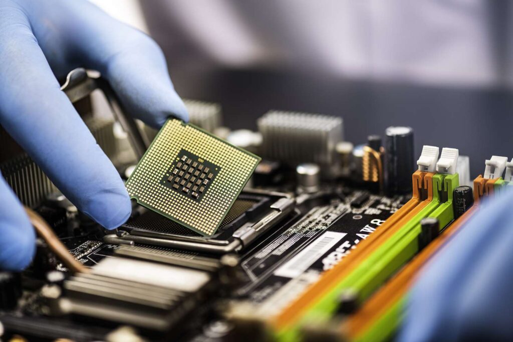
In the manufacture of integrated circuits, DC sputtering technology is used to deposit metal interconnect layers (such as aluminum, copper, etc.) to achieve electrical connections between different components inside the chip. In the manufacture of thin-film transistors, DC sputtering is used to deposit metal electrodes such as source, drain and gate, as well as insulating layers (such as aluminum oxide, silicon dioxide, etc.). In magnetic storage devices such as hard disk drives and magnetic tapes, DC sputtering technology is used to prepare magnetic films (such as cobalt-based alloys, iron-nickel alloys, etc.) to achieve high-density storage and stable reading of data. In the manufacture of various sensors (such as pressure sensors, temperature sensors, magnetic sensors, etc.), DC sputtering technology is used to deposit functional films such as sensitive layers, electrodes and insulating layers.
Optical Field
DC sputtering technology is widely used in the preparation of various optical films, such as anti-reflection films, high-reflection films, filters, etc. Anti-reflection films can reduce light reflection on the surface of optical components and improve light transmittance. They are often used in eyeglasses, camera lenses, etc. High-reflection films have high reflectivity for light of a specific wavelength and can be used for reflectors, laser resonators, etc. Filters can selectively transmit or absorb light of a specific wavelength and have important applications in spectral analysis, optical communications and other fields. Commonly used optical thin film materials include aluminum oxide, titanium oxide, zinc sulfide, etc. DC sputtering can accurately control the thickness and refractive index of the film to ensure the stability of optical performance.
Mechanical Manufacturing Field
DC sputtering technology can deposit wear-resistant, corrosion-resistant, and high-temperature resistant coatings on the surface of mechanical parts to improve the service life and performance of the parts. For example, sputtering titanium nitride (TiN) and titanium carbide (TiC) coatings on the surface of the tool can significantly improve the hardness and wear resistance of the tool; sputtering nickel-chromium alloys, titanium alloys, etc. coatings on the surface of wear-resistant parts such as bearings and gears can improve their wear and corrosion resistance. DC sputtering deposits hard coatings (such as titanium nitride, silicon carbide, etc.) on the mold surface, which can improve the surface hardness, wear resistance and demolding performance of the mold and reduce the maintenance cost of the mold.
Aerospace Field
The engine components and fuselage surfaces of aerospace vehicles work in harsh environments such as high temperature, high pressure, and corrosion. DC sputtering technology can deposit nickel-based high-temperature alloys, ceramic coatings (such as zirconium oxide), etc. to form thermal barrier coatings, which effectively protect components from high-temperature erosion. DC sputtering deposits titanium-aluminum alloys, magnesium-lithium alloys and other coatings on the surface of aircraft structural components, which can not only maintain the high strength of the components but also reduce weight. In aerospace electronic equipment, in order to prevent electromagnetic interference and ensure the normal operation of the equipment, electronic components and shells need to be electromagnetically shielded. DC sputtered copper, nickel and other metal coatings have good conductivity and can be used as electromagnetic shielding layers to effectively block the propagation of electromagnetic radiation.

Biomedical Field
On the surface of implantable medical devices such as artificial joints, dental implants, and heart stents, it is necessary to deposit a coating with good biocompatibility to promote tissue integration and reduce rejection. Titanium and titanium alloy coatings can form a good bond with human bone tissue after DC sputtering deposition, improving the stability and safety of implants. To prevent bacterial infection on the surface of medical devices and implants, DC sputtering technology can deposit coatings with antibacterial properties, such as silver coatings and zinc oxide coatings. These coatings can release antibacterial ions, inhibit the growth and reproduction of bacteria, and reduce the risk of infection.

Conclusion
DC sputtering technology is an important physical vapor deposition method with its advantages of simple equipment, low cost, high deposition rate, and good film uniformity. DC sputtering is compatible with a variety of metals, alloys, and some conductive compounds, and can produce films with different functions to meet the diverse needs of various industries for film performance. However, this technology also has certain limitations, such as being only applicable to conductive targets, prone to target poisoning, and internal stress in the film. In practical applications, it is necessary to optimize the process according to specific needs or use it in combination with other technologies.