The Ultimate Guide to Electron Beam Evaporation Coatings
From aerospace to semiconductors, electron beam evaporation technology stands out for its high deposition rate and excellent uniformity. Due to its efficient deposition of large-scale thin films, it has found widespread application in optics.
- Low Cost
- Good Film Uniformity
- Higher Film Deposition Rate
- Strong Film-Substrate Bonding
- Compatible With Conductive Materials
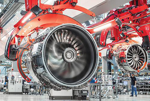
Wstitanium Workshop
Our Powerful Facilities
Everything You Should Know About Electron Beam Evaporation
Understanding the principles and processes of electron beam evaporation, as well as its diverse applications, is crucial for materials scientists and engineers. It not only helps optimize existing thin film deposition techniques and improve film quality and performance, but also provides a theoretical foundation and technical support for the development of new materials and applications. In the following articles, we will delve into various aspects of electron beam evaporation, demystifying this important technology.
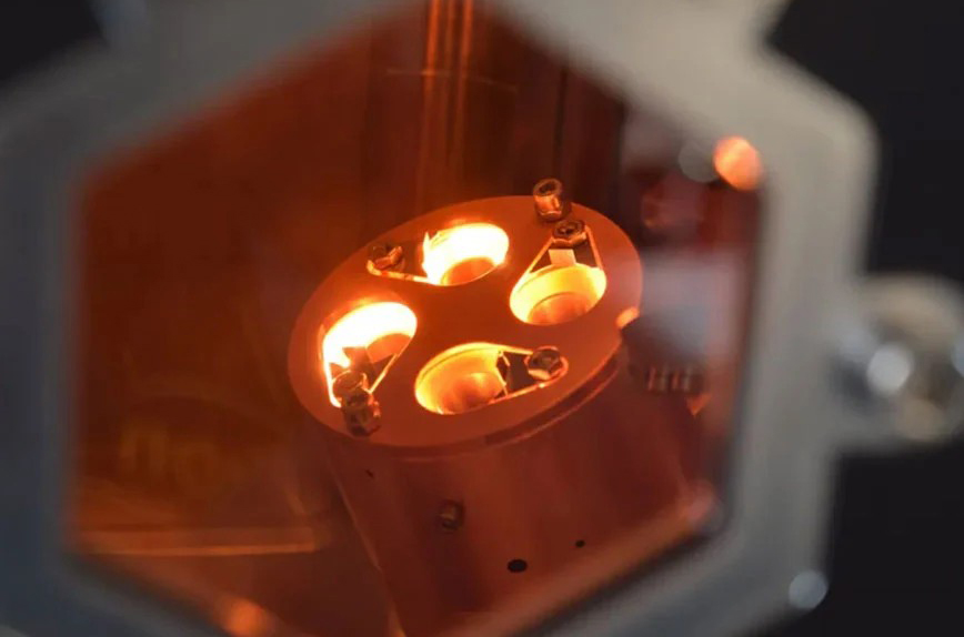
Electron beam evaporation is a key form of physical vapor deposition (PVD). Simply put, it involves bombarding the material to be evaporated with a high-energy electron beam in a high vacuum environment. This converts the kinetic energy of the electrons absorbed by the material into heat, thereby reaching the evaporation temperature. The evaporated gaseous atoms or molecules then freely fly in the vacuum and eventually deposit on the substrate surface, gradually accumulating to form a thin film (Thickness ranges from about 5 to 250 nanometers).
Technically, electron beam evaporation uses an electron gun to generate a high-energy electron beam. A hot cathode (typically a heated tungsten filament) within the gun emits thermal electrons. These electrons are accelerated by the high-voltage electric field generated by the accelerating anode, acquiring a high kinetic energy. The electron beam is then focused and guided by electromagnetic fields (including electrostatic and magnetic fields) to precisely impact the target material placed in a water-cooled crucible. Due to the highly concentrated energy of the electron beam, it can generate extremely high energy density within a very small area on the material surface, rapidly heating the material to the evaporation temperature and achieving efficient evaporation.

Principle of Electron Beam Evaporation
Electron beam evaporation begins with the generation and acceleration of electrons, a process carried out in an electron gun. The core component of the electron gun is a hot cathode, typically made of a tungsten filament. When current is applied to the tungsten filament, its temperature rises (Up to 2000 degrees Celsius), and the electrons within it gain sufficient energy to escape, a phenomenon known as thermionic emission.
The electrons’ energy is absorbed by the atoms of the evaporating material, causing them to gain sufficient energy to break free from their lattice positions and enter an excited or ionized state. As more and more atoms gain energy, the atoms on the surface of the material begin to overcome the interatomic bonds and gradually transition from a solid state to a gaseous state, thus causing evaporation. The energy density of the electron beam has a critical influence on the evaporation rate. The higher the energy density, the more energy is delivered to the evaporating material per unit time, resulting in a faster evaporation rate. By adjusting the current and voltage of the electron gun, the electron beam energy density can be precisely controlled, thereby achieving precise control of the evaporation rate.
There is a concentration gradient between the evaporation source (the evaporating material bombarded by the electron beam) and the substrate. According to the principle of diffusion, the evaporating atoms diffuse from the high-concentration evaporation source to the low-concentration substrate. To ensure uniform deposition of evaporated atoms on the substrate surface, auxiliary devices such as baffles and masks are typically incorporated into the equipment to control the transport path and distribution of the evaporated atoms. Ion beam bombardment increases the mobility of the evaporated atoms on the substrate surface, resulting in denser film crystals and improved hardness, adhesion, and electrical properties.
Materials For Electron Beam Evaporation
Electron beam evaporation can deposit a wide variety of coating types onto a variety of substrates. While this is not an exhaustive list of materials that can be evaporated using electron beam evaporation, some typical evaporation materials and substrate materials are listed below.
Evaporation Material
The evaporation material is the raw material placed in the crucible and serves as the target for the electron beam. Electron beam evaporation offers the widest range of material compatibility due to its ability to reach higher temperatures. For example, electron beam evaporation is well-suited for coating metals and dielectric materials with higher melting points, such as aluminum, copper, nickel, titanium tin, chromium, gold, silver, platinum, tungsten, and tantalum, as well as indium tin oxide and silicon dioxide.
Substrate Materials
Thin films are applied to a variety of substrates. Silicon, quartz, and sapphire wafers are common in electronics. Other possible substrates include ceramics such as silicon nitride and glass.
| Evaporation Material | Substrates |
| Metals: Gold (Au), Silver (Ag), Copper (Cu), Nickel (Ni), Titanium (Ti), Chromium (Cr) | Silicon Wafers: Common in semiconductor and microelectronics applications. |
| Refractory Metals: Tungsten (W), Tantalum (Ta) | Glass, Ceramics, and Quartz: Used for optical coatings and decorative films. |
| Dielectrics: Indium Tin Oxide (ITO), Silicon Dioxide (SiO2), Magnesium Fluoride (MgF2) | Sapphire: Ideal for high-performance optical components and LEDs |
E-Beam Evaporation vs. Other PVD Techniques
| Criteria | E-Beam Evaporation vs. Thermal Evaporation | E-Beam Evaporation vs. Sputtering |
| Deposition Rate | Higher in E-Beam Evaporation compared to Thermal Evaporation. | Higher in E-Beam Evaporation compared to Sputtering. |
| Material Compatibility | E-Beam Evaporation can handle high-melting-point materials like metal oxides. | Sputtering is more effective for coating complex geometries and large-area substrates, while E-Beam Evaporation is optimized for line-of-sight deposition. |
| Film Density | E-Beam Evaporation produces denser thin films with fewer impurities. | E-Beam Evaporation results in in films with higher density compared to sputtering, especially when the material has a high melting point. This is because the vaporized material is generally in a neutral atomic or molecular state, leading to a more compact and dense film structure as the particles condense directly onto the substrate. |
| Heating Method | E-beam uses a high-power electron beam to directly heat the material. Thermal evaporation uses an electric current to heat the crucible. | Unlike E-Beam Evaporation, sputtering uses plasma atoms (typically argon) to dislodge material from a negatively charged target. |
| Purity | E-beam has higher purity due to minimized contamination from the crucible. | E-Beam Evaporation typically provides higher purity than Sputtering. |
Advantages of Electron Beam Evaporation Coating
High-Purity Thin Film Production Capabilities
The evaporation material is placed in a water-cooled crucible, and the electron beam bombards only a localized area of the evaporating material. Since most of the evaporating material is kept at a low temperature, chemical reactions between the evaporating material and the crucible are virtually nonexistent, effectively preventing crucible contamination.
Widely Compatible Materials
Due to the extremely high energy generated by the electron beam, it can evaporate nearly all types of materials, including high-melting-point metals (such as tungsten, molybdenum, and tantalum), alloys, oxides (such as silicon dioxide, aluminum oxide, and tantalum pentoxide), sulfides (such as zinc sulfide), and fluorides (such as magnesium fluoride).
Precise Control
Precisely adjusting parameters such as the electron gun voltage and current allows for flexible and precise control of the electron beam energy and beam intensity, enabling precise regulation of the evaporation rate of the evaporating material.
Higher Deposition Rate
Increasing the electron beam power significantly increases the evaporation rate of the evaporation material, enabling the deposition of thicker films in a shorter time. This improves production efficiency.
Disadvantages of Electron Beam Evaporation
High Equipment Cost
Electron beam evaporation equipment consists of multiple complex and precise components, such as the electron gun, vacuum system, electromagnetic focusing and deflection device, water cooling system, and control system. High equipment costs can be a barrier to electron beam evaporation technology.
Poor Thin Film Uniformity
Evaporated atoms escape in a cosine-distributed pattern. The deposition rate of atoms varies significantly at different locations on the substrate. The deposition rate is lower at the center of the substrate, while it is higher at the edges, which can easily lead to uneven deposition.
Parameter Control is Difficult
Electron beam evaporation involves voltage, current, focus and deflection, the temperature of the evaporating material, the vacuum level, and the substrate temperature. Even the slightest fluctuation in any of these parameters can significantly affect the quality of the thin film.
Prone to Waste
Electron beam evaporation places extremely stringent demands on the purity of the target material. Due to the highly concentrated energy of the electron beam, it can easily lead to localized overheating of the target surface, resulting in ineffective evaporation and deposition of some target material, resulting in waste.
Applications of Electron Beam Evaporation
Electron beam evaporation has driven technological advancements and innovations in numerous fields, including semiconductors and microelectronics, optics, data storage, aerospace, and biomedicine. In semiconductor manufacturing, it is a key technology for achieving high-performance chip production. In optics, it provides technical support for the manufacture of various precision optical components. In data storage, it helps push the limits of storage density and read/write speeds. In aerospace, it ensures the performance and safety of aircraft in extreme environments. In biomedicine, it provides new means and methods for disease diagnosis and treatment.
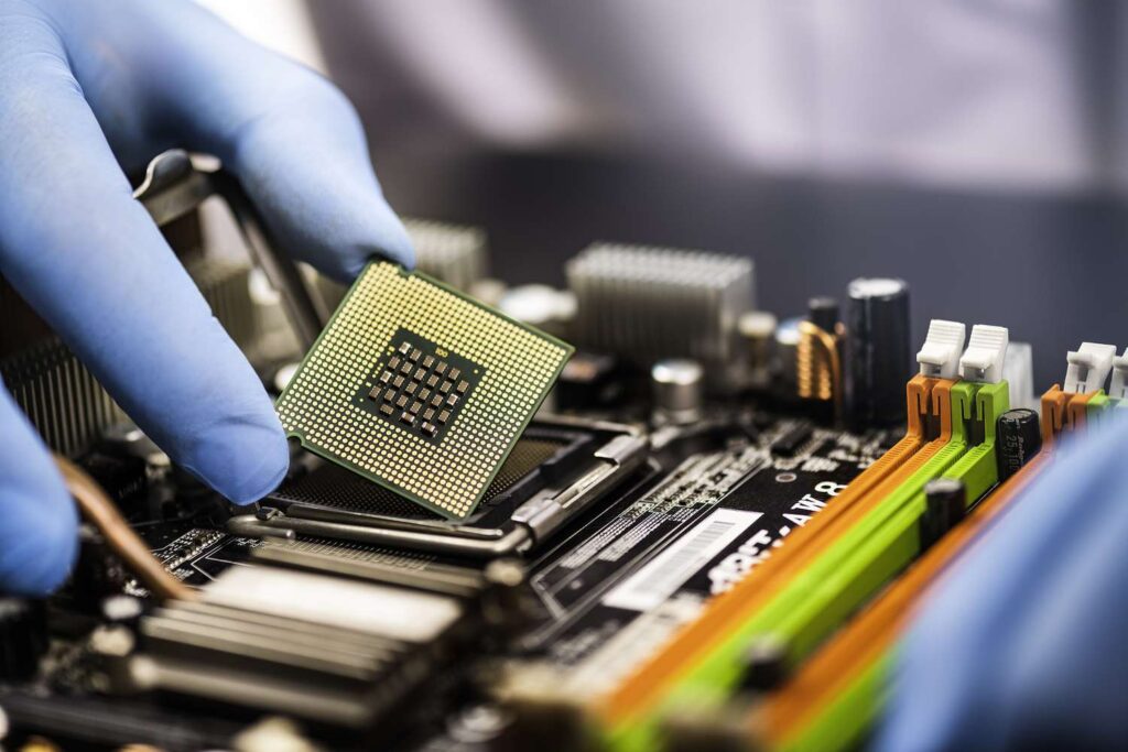
Semiconductors
In semiconductor device manufacturing, electron beam evaporation is commonly used to form metal electrodes and interconnect layers. For example, in integrated circuits, electron beam evaporation is used to deposit thin metal films such as aluminum and copper to serve as the source, drain, and gate electrodes of transistors. In some advanced semiconductors, electron beam evaporation is also used to deposit specialized diffusion layers. For example, in CMOS (complementary metal oxide semiconductor) devices, precise control of the thickness and composition of the diffusion layer can optimize the threshold voltage and switching speed of the transistor, improving overall chip performance.
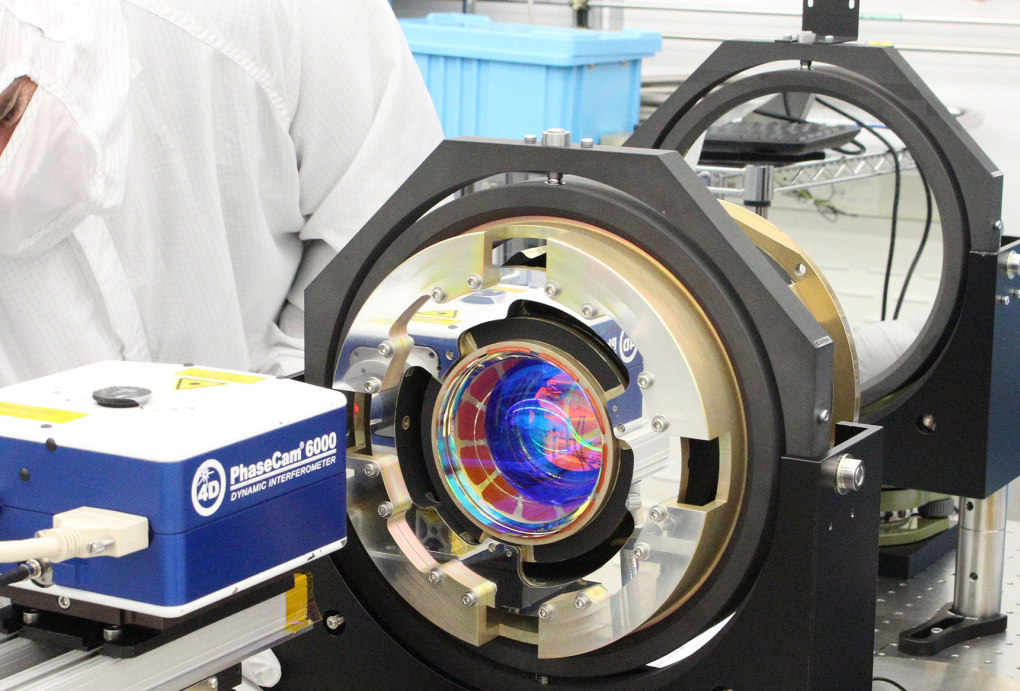
Optics
Electron beam evaporation is a key technology for preparing various optical thin films, widely used in the manufacture of optical components such as lenses, mirrors, and filters. By precisely controlling the thickness and refractive index of the film and leveraging the principle of light interference, it can be used to create antireflection coatings, which reduce reflection losses on the surface of optical components, improve light transmittance, and enhance image clarity. Highly reflective films can be used to enhance the reflection of specific wavelengths of light, for applications such as laser mirrors and telescope mirrors. Bandpass filters and cutoff filters can be used to selectively transmit or cutoff specific wavelengths of light, meeting the optical performance requirements of optical instruments in various application scenarios.
Data Storage
Electron beam evaporation is used to create high-performance magnetic films in the manufacture of data storage media such as hard disks and magnetic tapes. By precisely controlling the composition, thickness, and microstructure of magnetic films, magnetic properties such as coercivity, remanence, and permeability can be optimized, thereby increasing data storage density and read/write speeds. For example, in perpendicular magnetic recording hard disks, magnetic films such as cobalt platinum (CoPt) created using electron beam evaporation exhibit high magnetic anisotropy, enabling higher-density data storage, meeting the growing demand for massive data storage and driving the development of data storage technology towards higher capacity and faster read/write speeds.
Aerospace
Components such as aircraft engines and spacecraft thermal protection systems operate in high temperatures, high airflows, and harsh environments, requiring high-temperature resistance, oxidation resistance, and corrosion resistance. Electron beam evaporation can deposit ceramic coatings (such as alumina and yttria-stabilized zirconia) and metal alloy coatings (such as nickel-based and cobalt-based superalloys) on the surfaces of these components, forming a strong protective layer that effectively protects the component base material, improves component strength and oxidation resistance in high-temperature environments, extends component service life, and ensures safe and reliable operation of aerospace equipment under extreme operating conditions.
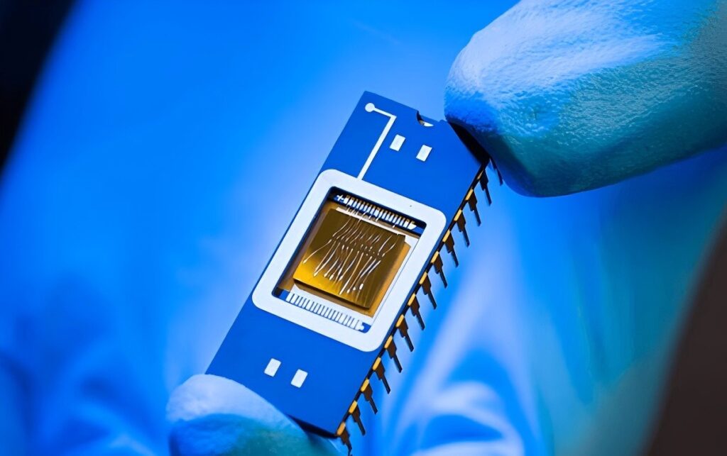
Biomedicine
In the fabrication of biosensors, electron beam evaporation can be used to deposit metal thin films (such as gold and platinum) as electrode materials. Biocompatible thin films (such as parylene and titanium dioxide) can be prepared as carriers for immobilizing biomolecules and protective layers on sensor surfaces. These thin films can precisely control their thickness and surface properties, improving the biosensor’s recognition and sensitivity for biomolecules, enabling rapid and accurate detection of biomarkers.
Implants such as artificial joints and cardiac stents require excellent compatibility with human tissue while also exhibiting wear and corrosion resistance. Electron beam evaporation can deposit bioactive ceramic films (such as hydroxyapatite) and corrosion-resistant metal films (such as titanium alloys) on implant surfaces, improving their biocompatibility and promoting cell adhesion.

Conclusion
Electron beam evaporation, as an important physical vapor deposition technology, plays an indispensable role in modern materials science and industrial production. In principle, it uses a high-energy electron beam to bombard the evaporated material, transforming it from a solid to a gaseous state and depositing it as a film on a substrate. This unique energy and material transfer mechanism endows the technology with numerous advantages. Electron beam evaporation can produce high-purity thin films, meeting the demands of fields such as semiconductors and optics, which require extremely high material purity. It can evaporate a wide range of materials, addressing the difficulty of evaporating high-melting-point materials. Its precise evaporation rate and film thickness control make it an excellent choice for producing films with specific properties and dimensions. Its high deposition rate improves production efficiency and reduces costs in industrial production.