The Ultimate Guide to Ion Beam Sputtering
The application of ion beam sputtering technology in the fields of semiconductors, optics, data storage, etc. continues to expand and deepen. Especially in semiconductor manufacturing, ion beam sputtering technology plays a key role in improving chip performance and miniaturizing size.
- High Film Quality
- Low Temperature
- Wide Range of Materials
- Precise Parameter Control
Wstitanium Workshop
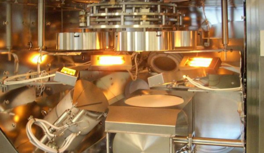
Our Powerful Facilities
Everything You Should Know About Ion Beam Sputtering
Ion beam sputtering (IBS) has become a key technology in many scientific research and industrial applications due to its unique advantages. From precision coating of optical components to the manufacture of semiconductor devices. Understanding the principles, processes, classifications and applications of ion beam sputtering technology in different fields is of great significance for researchers and engineers engaged in related fields such as materials science, electronic engineering, and optical engineering. This blog will comprehensively and in-depth explore ion beam sputtering technology and present you with a complete knowledge system about ion beam sputtering.
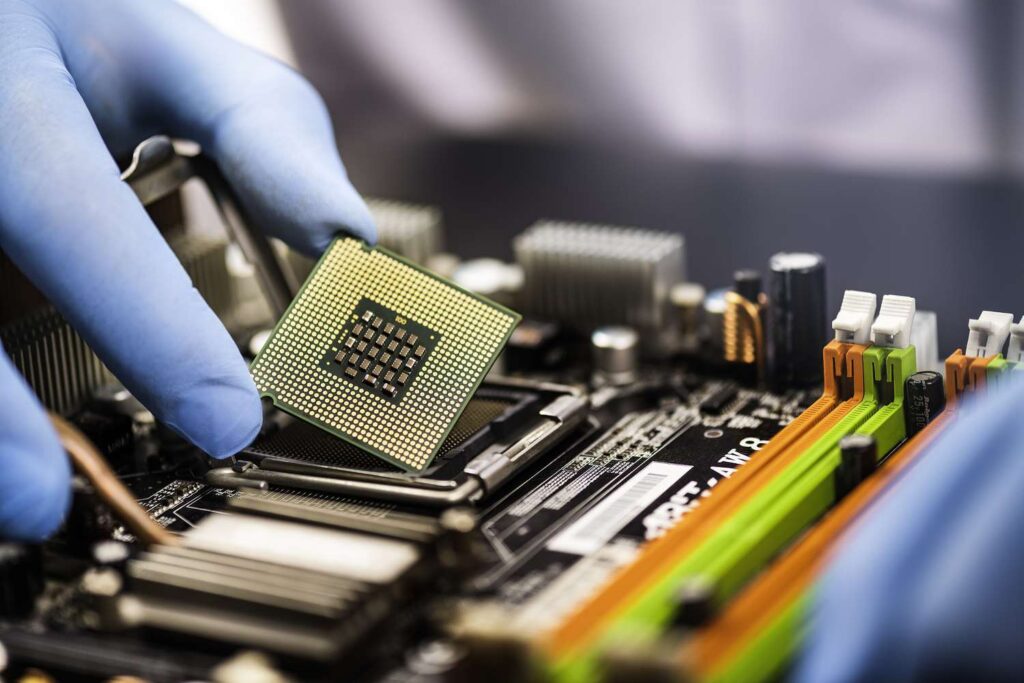
Ion beam sputtering, also known as ion beam deposition or ion beam sputtering deposition (IBSD), is a type of physical vapor deposition (PVD) technology. The basic principle is to bombard the target surface with a focused high-energy ion beam (usually inert gas ions, such as argon ions) in a vacuum environment. These high-energy ions collide with the target atoms, and through energy transfer, the target atoms obtain enough energy to overcome the surface binding force, and are sputtered from the target surface. The sputtered atoms or molecules fly freely in the vacuum and eventually deposit on the substrate surface to form a uniform and dense film. The core of ion beam sputtering is to accurately control the energy, beam current density and type of ions of the ion beam to achieve precise regulation of the film growth process, thereby obtaining a film with specific properties and structure.

Working principle of ion beam sputtering
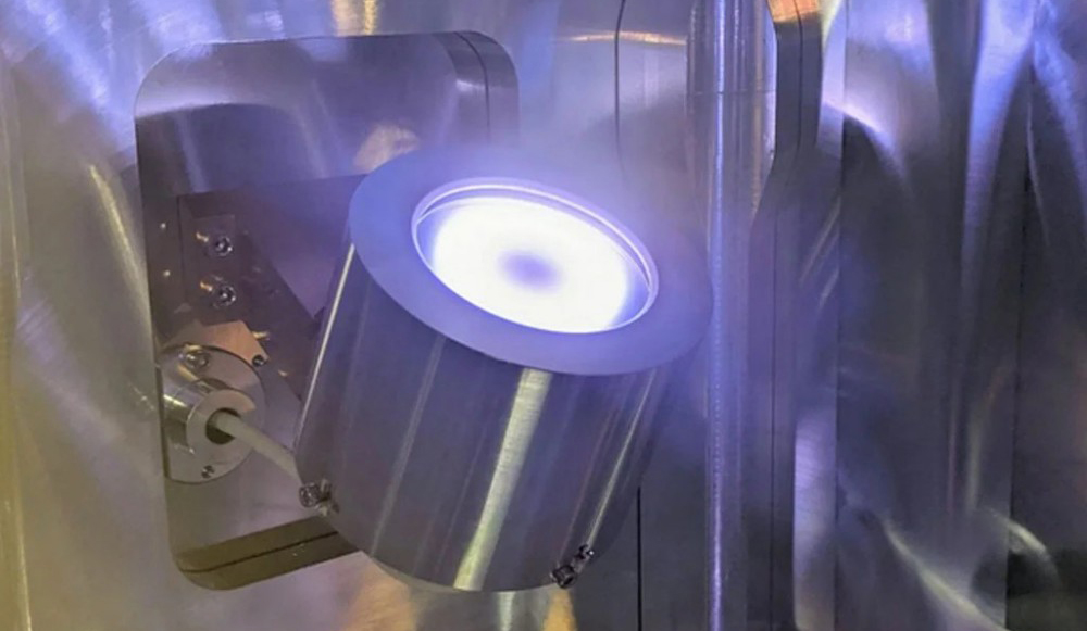
The ion source is one of the key components of the ion beam sputtering system, and its function is to create a high-energy ion beam. Common ion sources include radio frequency ion sources, electron bombardment ion sources, etc. Taking the radio frequency ion source as an example, under the action of the radio frequency electric field, the inert gas (such as argon) is ionized into a plasma, which contains a large number of ions and electrons. Through the action of a series of electric and magnetic fields, these ions are accelerated and focused to form an ion beam with a certain energy and beam density, and then directed to the target material.
When a high-energy ion beam bombards the surface of the target material, the ions and the target atoms undergo elastic and inelastic collisions. In elastic collisions, ions transfer part of their kinetic energy to the target atoms, causing the target atoms to gain energy and then displace in the lattice; in inelastic collisions, charge transfer and other processes may occur between ions and target atoms. When the energy obtained by the target atoms is large enough to exceed their binding energy on the target surface, they will be sputtered from the target surface to form sputtered atoms. The energy and direction of sputtered atoms have a certain distribution, which is related to factors such as the energy of the ions, the angle of incidence, and the properties of the target.
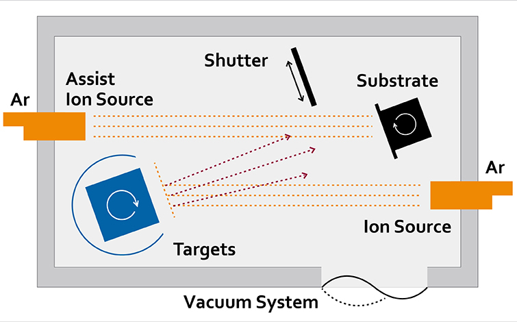
The atoms sputtered from the target surface fly in all directions at a certain speed in a vacuum. Since the substrate is placed near the target and is usually grounded or has a certain bias, the sputtered atoms will be affected by the electric field during flight and eventually deposited on the substrate surface. During deposition, the sputtered atoms will diffuse and migrate on the substrate surface, combine with the deposited atoms, and gradually form a thin film. The growth process of the film is affected by many factors, such as the energy of the sputtered atoms, the substrate temperature, the deposition rate, etc. These factors determine the structure, performance and quality of the film.
The Process of Ion Beam Sputtering
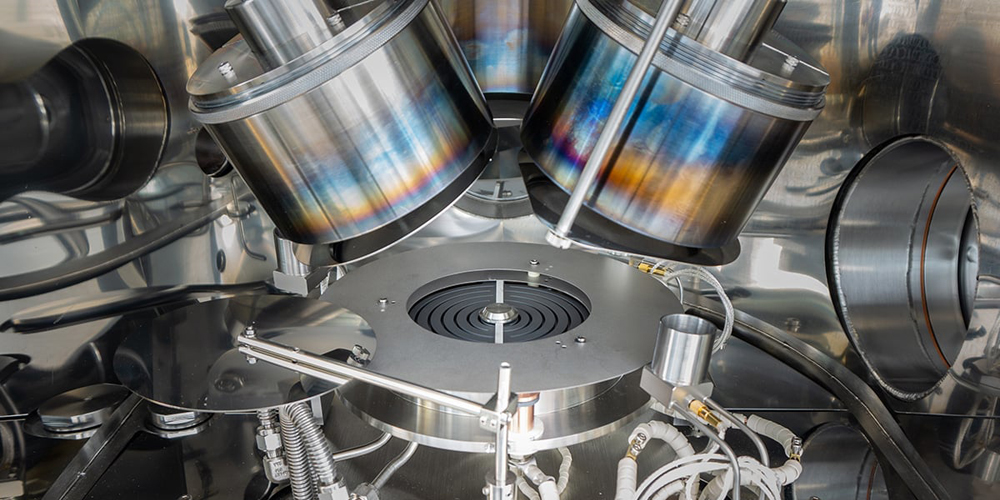
Ion beam sputtering needs to be carried out in a high vacuum environment to avoid collisions between sputtered atoms and gas molecules in the air, which will affect the quality and purity of the film. Before starting sputtering, you first need to use a vacuum pump group (such as a mechanical pump, diffusion pump, molecular pump, etc.) to evacuate the sputtering chamber and reduce the air pressure in the chamber to 10⁻⁴ Pa or even lower. Only in a high vacuum environment can the ion beam be transmitted stably and the sputtered atoms can be smoothly deposited on the substrate to form a high-quality film.
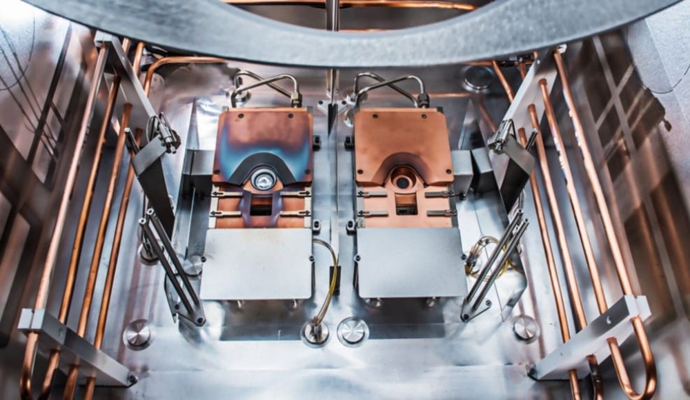
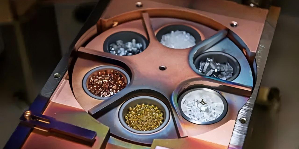
Preparation of Target and Substrate
Selecting a suitable target is one of the key steps in ion beam sputtering. The material of the target should be the same as the material of the film to be prepared. The target usually needs to be precisely manufactured to ensure its surface flatness and finish to improve the sputtering efficiency and the uniformity of the film. For the substrate, strict cleaning and pretreatment are also required to remove impurities, oil stains and oxides on the surface to enhance the adhesion between the film and the substrate. Factors such as the material, surface state and temperature of the substrate will have an important impact on the growth and performance of the film.
Ion Beam Parameters
In ion beam sputtering, it is necessary to precisely adjust the various parameters of the ion beam to achieve precise control of film growth. These parameters include ion energy, beam density, ion incident angle, etc. Ion energy determines the energy and sputtering yield of sputtered atoms. Ion energy can be changed by adjusting the acceleration voltage of the ion source; beam density affects the deposition rate of the film, which can be controlled by adjusting the working current of the ion source or using a beam controller; ion incident angle affects the distribution of sputtered atoms and the growth direction of the film, and the ion incident angle can be changed by adjusting the relative position between the ion source and the target material and the substrate.
Deposition and Monitoring
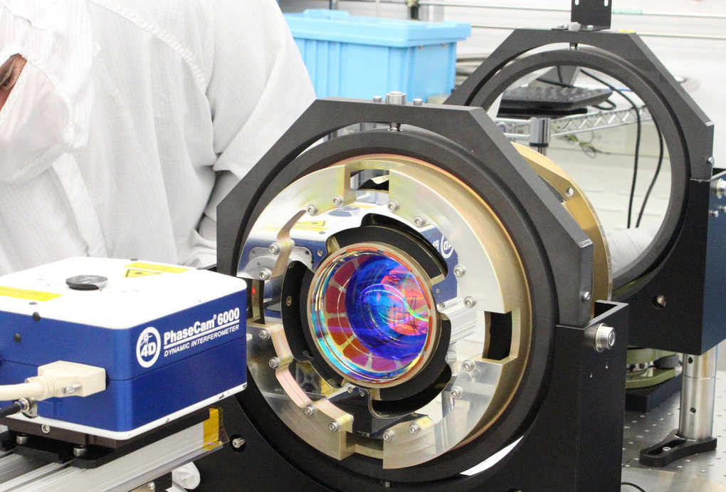
When the ion beam bombards the target material and the sputtered atoms begin to deposit on the substrate, the growth of the film needs to be monitored in real time. Common monitoring methods include quartz crystal microbalance (QCM), optical interferometry, etc. QCM monitors the deposition thickness of the film in real time by measuring the change in the oscillation frequency of the quartz crystal; the optical interferometry law uses the interference principle of light to determine the thickness and refractive index of the film by measuring the change in the interference fringes of the reflected light or the transmitted light. Through these monitoring methods, sputtering parameters can be adjusted in time to ensure that the thickness, uniformity and quality of the film meet the requirements. After the film deposition is completed, a series of characterization and testing of the film is required, such as scanning electron microscopy (SEM) to observe the surface morphology and cross-sectional structure of the film, X-ray diffraction (XRD) to analyze the crystal structure of the film, and energy spectrum analysis (EDS) to determine the chemical composition of the film, in order to comprehensively evaluate the performance of the film.
Classification of Ion Beam Sputtering
Single Ion Beam Sputtering
Single ion beam sputtering is the most basic ion beam sputtering, where only one ion source generates an ion beam to bombard the target. The structure is relatively simple and easy to operate, and it is suitable for some application scenarios that do not have particularly strict requirements on film performance, such as ordinary metal film preparation, surface modification, etc.
Dual Ion Beam Sputtering
Dual ion beam sputtering adds an auxiliary ion source on the basis of single ion beam sputtering. One of the ion beams is used to bombard the target material to produce sputtered atoms; the other auxiliary ion beam directly bombards the surface of the growing film. Dual ion beam sputtering is suitable for the preparation of high-quality optical films, semiconductor films, etc.
Reactive Ion Beam Sputtering
Reactive ion beam sputtering is to introduce reactive gas (such as oxygen, nitrogen, etc.) into the sputtering chamber. The reactive gas reacts chemically with the sputtered target atoms on the surface of the substrate to form a compound film. Reactive ion beam sputtering provides an effective method for preparing various compound films. Such as magnetic films.
When to Use Ion Beam Sputtering
High Requirements for Film Quality
In the field of optics, such as the preparation of high-power laser reflectors and optical filters, the optical properties (such as low scattering, low absorption, high laser damage threshold) and uniformity of the film are extremely high.
Thin films of special materials
For some materials with high melting points and low vapor pressures, it is difficult to prepare thin films by evaporation coating. Ion beam sputtering sputters these materials from the target surface and deposits them into films through the bombardment of high-energy ions.
Precise control of film growth
Ion beam sputtering achieves precise control of film growth rate, atomic migration, crystal orientation and other growth. This precise control capability makes ion beam sputtering an important tool for studying the growth mechanism of thin films.
Advantages of Ion Beam Sputtering
High film quality
The film prepared by ion beam sputtering has extremely high density and uniformity, and few internal defects in the film. This is because the sputtered atoms have high energy and can fully diffuse and migrate when deposited on the substrate surface, tightly combining with the deposited atoms to form a dense film structure
Precise parameter control
Ion beam sputtering technology accurately controls parameters such as ion energy, beam density, and incident angle, thereby achieving precise regulation of film growth rate, composition, structure, and performance. Films of different thicknesses, different composition gradients, and different crystal structures are prepared.
Wide range of materials
Ion beam sputtering is compatible with any material, including metals, semiconductors, insulators, compounds, etc. Whether it is a metal with a high melting point (such as tungsten and molybdenum) or a material with a low vapor pressure, it can be successfully prepared into a thin film by ion beam sputtering.
Low temperature
Compared with some other thin film preparation methods (such as chemical vapor deposition, CVD), ion beam sputtering can usually be carried out at a lower temperature. This is very beneficial for some temperature-sensitive substrate materials (such as plastics, organic materials, etc.).
Advantages of Ion Beam Sputtering
High equipment cost
Ion beam sputtering systems usually include multiple complex components such as ion sources, vacuum systems, target and substrate mounting devices, and control systems. The equipment is difficult to manufacture, so the cost is relatively high.
Low deposition rate
Compared with some other physical vapor deposition methods (such as evaporation coating, magnetron sputtering, etc.), the deposition rate of ion beam sputtering is relatively low. This is because the number of atoms sputtered out and deposited on the substrate per unit time is small.
Low target utilization
In ion beam sputtering, the bombardment of the ion beam is mainly concentrated on the local area of the target surface, resulting in uneven sputtering of the target. Only part of the target is effectively sputtered, and the target utilization rate is relatively low. This not only causes a waste of target resources, but also increases production costs.
Ion Beam Sputtering vs. Evaporation Coating
Evaporation coating is to evaporate the target material by heating, and then condense and deposit on the substrate surface to form a thin film; while ion beam sputtering uses high-energy ions to bombard the target material, so that the target atoms are sputtered out and deposited on the substrate. The film prepared by evaporation coating usually has a higher purity. Due to the low energy of the evaporated atoms, the density and adhesion of the film are relatively poor. The film prepared by ion beam sputtering has high density, strong adhesion and good uniformity. Evaporation coating is suitable for materials with low melting points and easy evaporation; ion beam sputtering is suitable for almost all materials, including materials with high melting points and difficult to evaporate.
Ion Beam Sputtering vs. Magnetron Sputtering
Magnetron sputtering is to apply a magnetic field to the surface of the sputtering target, use the magnetic field to constrain the movement of electrons, increase the plasma density, and thus improve the sputtering efficiency; ion beam sputtering is to generate an ion beam bombarding the target material through an independent ion source. Both magnetron sputtering and ion beam sputtering can produce high-quality films. Ion beam sputtering has advantages in film uniformity and precise control of film growth. The deposition rate of magnetron sputtering is usually higher than that of ion beam sputtering, and it is more suitable for large-scale production. Magnetron sputtering equipment is relatively simple and low-cost; ion beam sputtering equipment is complex and high-cost.
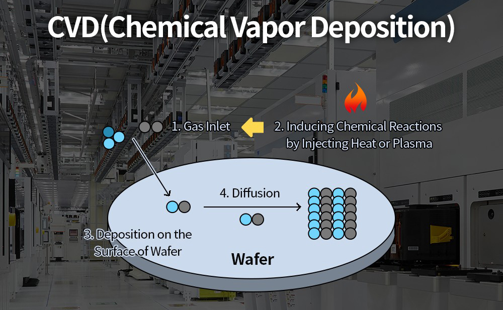
Ion Beam Sputtering vs. Chemical Vapor Deposition
CVD uses gaseous chemicals to react chemically on the surface of the substrate to generate solid thin film materials; ion beam sputtering is a physical process and does not involve chemical reactions. CVD can produce thin films with good stoichiometric ratios and crystal structures, but may introduce some chemical impurities; thin films prepared by ion beam sputtering are high in purity and have few defects. CVD usually requires a higher deposition temperature, which may affect the performance of the substrate and film; ion beam sputtering can be carried out at a lower temperature and is suitable for temperature-sensitive materials. CVD equipment is relatively complex and requires precise control of multiple parameters such as the flow rate, temperature, and pressure of the reaction gas; ion beam sputtering equipment mainly focuses on the control of the ion source and vacuum system.
Application of Ion Beam Sputtering
As an advanced physical vapor deposition technology, ion beam sputtering plays an irreplaceable role in many fields such as optics, semiconductors, data storage, protective coatings, and biomedicine due to its unique advantages in film quality, process control, and material applicability.
Optics
In laser optical systems, high-reflectivity mirrors and low-reflectivity anti-reflection films are required. The thin films prepared by ion beam sputtering have extremely low scattering and absorption characteristics, which can meet the strict requirements of high-power laser systems for optical components. By precisely controlling the thickness and refractive index of the film, optical films with high or low reflectivity in a specific wavelength range are prepared, which are widely used in laser resonators, laser amplifiers, optical imaging systems, etc. Ion beam sputtering technology can also prepare various types of optical filters, such as bandpass filters, long-wave pass filters, short-wave pass filters, etc.
Semiconductors
In integrated circuit manufacturing, ion beam sputtering is used to prepare key films such as metal interconnect layers, gate materials, and barrier layers. Since ion beam sputtering can precisely control the thickness and composition of the film and can be carried out at low temperatures, it will not have a negative impact on the performance of semiconductor devices. Ion beam sputtering sputters a layer of insulating film or doped film on the surface of the semiconductor to adjust the surface charge distribution, carrier concentration and other parameters of the semiconductor, thereby improving the performance and stability of the device.
Sensors
Magnetoresistive sensors are widely used in automotive electronics, industrial control, consumer electronics and other fields, and their core is magnetoresistive film. Ion beam sputtering technology can produce magnetoresistive films with high magnetoresistance and low noise, such as giant magnetoresistance (GMR) film and tunnel magnetoresistance (TMR) film. The performance of these films directly affects the sensitivity and accuracy of the sensor. The precise control capability of ion beam sputtering ensures the stability and consistency of film performance, providing reliable technical support for the manufacture of high-performance magnetoresistive sensors.
Biomedicine
Preparing biocompatible films on the surface of medical devices (such as artificial joints, heart stents, dental implants, etc.) can improve their compatibility with human tissues and reduce rejection reactions. Ion beam sputtering can produce biocompatible films such as hydroxyapatite (HA) and titanium oxide (TiO₂). HA film is similar to the composition of human bones, which can promote the growth and attachment of bone cells and improve the stability of artificial bone implants; TiO₂ film has good biological inertness and blood compatibility, and is often used in heart stents, etc.

Conclusion
The core of ion beam sputtering is to achieve precise control of film growth by bombarding the target material with high-energy ion beams, thereby preparing high-quality films with specific properties and structures. From the perspective of technical characteristics, ion beam sputtering can produce dense, uniform, and defect-free films, and can accurately control the composition, thickness, and structure of the film. It is suitable for the preparation of films of various materials (including high melting points, special compounds, etc.), and has the advantages of low-temperature processes and is friendly to temperature-sensitive substrates. However, this technology also has shortcomings such as high equipment cost, low deposition rate, and low target material utilization, which to a certain extent limit its large-scale application.