The Ultimate Guide to Low Pressure Chemical Vapor Deposition
A deep understanding of the principles, applications, and advantages of LPCVD is crucial for understanding development trends in materials science and semiconductor manufacturing. We will comprehensively and in-depth explore various aspects of low-pressure chemical vapor deposition technology.
- Good Film Uniformity
- Higher Film Deposition Rate
- Strong Film-Substrate Bonding
- Compatible With Conductive Materials
Everything You Should Know About LPCVD
Low-pressure chemical vapor deposition (LPCVD), a highly precise and widely used thin-film deposition method, has achieved remarkable development over the past few decades and plays an indispensable role in numerous key technological fields. As electronic devices continue to evolve towards miniaturization and higher performance, the requirements for the surface properties of semiconductor devices and various materials are becoming increasingly stringent. For example, in chip manufacturing, achieving higher integration and faster operating speeds requires depositing high-quality, uniform thin films with precisely controlled thickness within extremely small spaces to construct complex circuit structures. LPCVD technology, with its unique advantages in meeting these high-precision requirements, has become a core technology in semiconductor manufacturing.
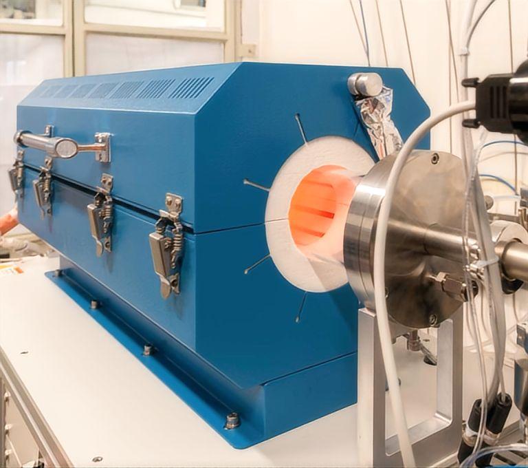
Low-pressure chemical vapor deposition (LPCVD) is a variant of chemical vapor deposition (CVD). CVD involves the use of gaseous chemicals to react on a solid surface, producing a solid deposit. LPCVD is performed under low pressure, typically between 0.1 and 10 Torr, significantly lower than standard atmospheric pressure (760 Torr). In LPCVD, one or more gaseous precursors are introduced into a vacuum chamber. Under specific temperature and pressure conditions, these precursors react on the substrate surface, and the reaction products gradually deposit onto the substrate, forming a thin, solid film. For example, when depositing silicon thin films, silane (SiH₄) is often used as a gaseous precursor. Under certain conditions, silane decomposes, depositing silicon atoms on the substrate surface to form the silicon film, while also producing hydrogen and other byproducts.

Principle and Procedure
Gas Delivery: Gaseous precursors are introduced into the reaction chamber using precisely controlled devices such as mass flow controllers. Because the reaction occurs at low pressure, the mean free path of the gas molecules is increased, allowing the gas to be more evenly distributed within the reaction chamber, creating favorable conditions for subsequent reactions on the substrate surface. For example, when depositing silicon nitride thin films, gaseous precursors such as silane and ammonia are delivered to the reaction chamber at a specific ratio and flow rate.
Adsorption: Upon reaching the substrate surface, gaseous precursor molecules adhere to the substrate through physical adsorption or chemical adsorption. Physical adsorption is based on intermolecular van der Waals forces and is weak and reversible; chemical adsorption involves a chemical reaction between the molecules and the substrate surface, forming a chemical bond and resulting in a stronger bond. The adsorption process is influenced by various factors, including temperature, pressure, and substrate surface properties.
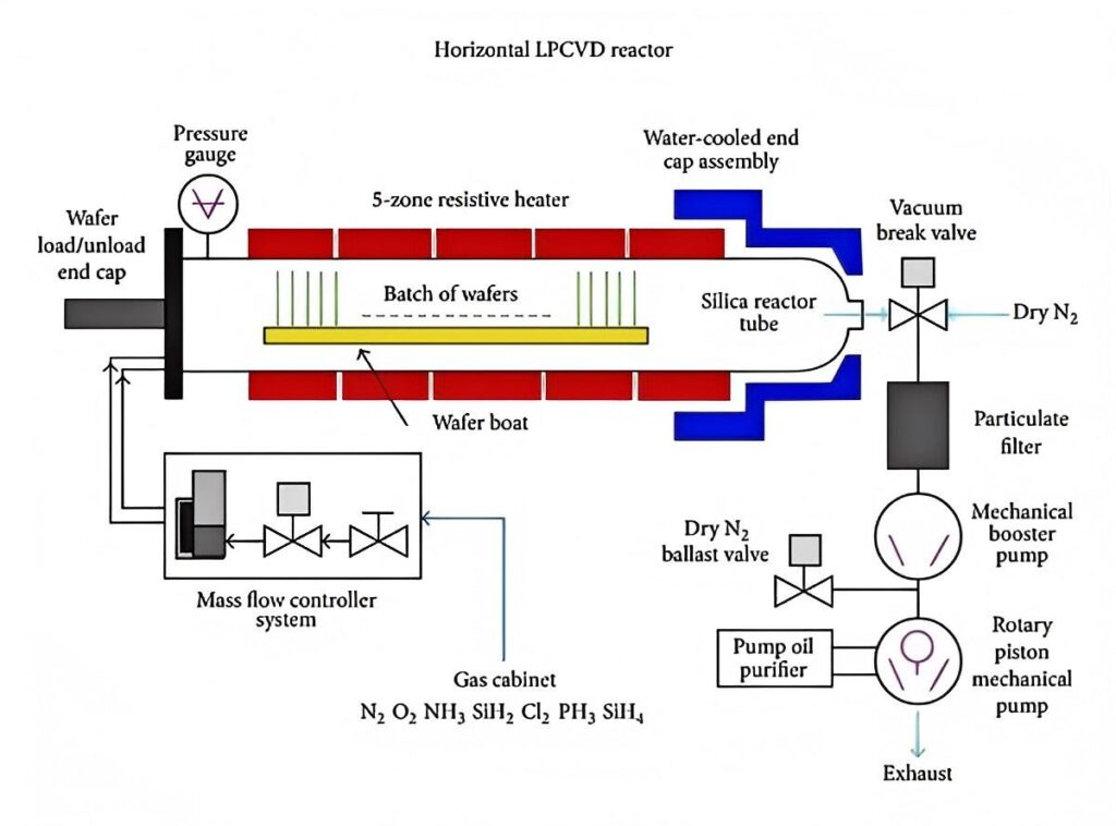
Reaction: Precursor molecules adsorbed on the substrate surface undergo a chemical reaction at a set temperature. These reactions can be decomposition, replacement, or redox reactions, depending on the precursor used and the film material being deposited. For example, when depositing a silicon dioxide film, silane (SiH₄) and oxygen (O₂) react: SiH₄ + O₂ → SiO₂ + 2H₂, forming a silicon dioxide film on the substrate surface.
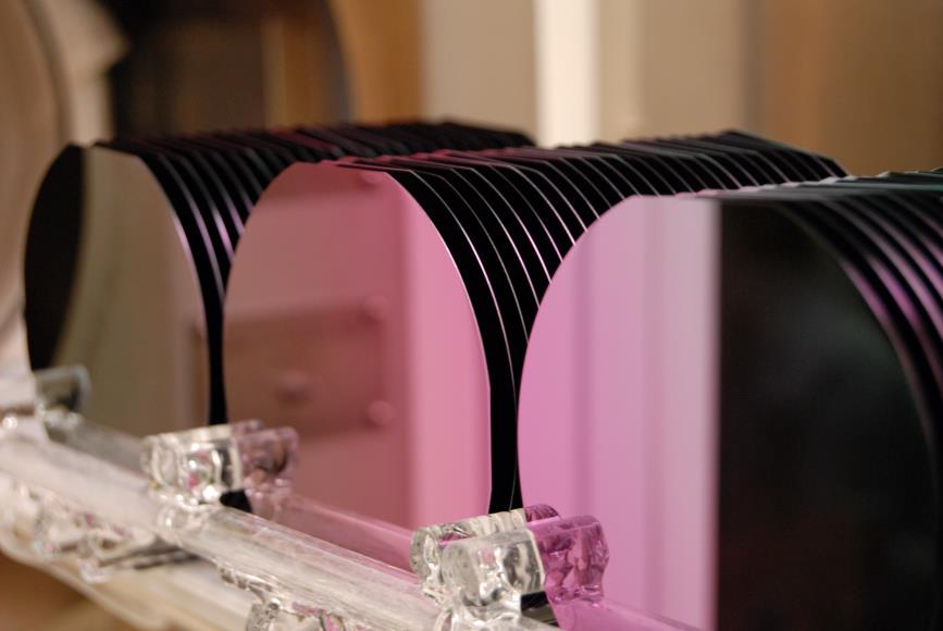
Deposition: The solid products produced by the reaction gradually accumulate on the substrate surface, forming a continuous film. As the reaction continues, the film thickness increases. During deposition, the film growth rate, uniformity, and quality are influenced by a combination of factors, including precursor concentration, reaction temperature, pressure, and reaction time.
Byproduct Removal: Gaseous byproducts are produced during the reaction, such as hydrogen in the aforementioned reaction. These byproducts must be promptly removed from the reaction chamber to prevent them from re-entering the reaction or contaminating the deposited film. The by-products are pumped out of the reaction chamber by means of a vacuum pump and other equipment to maintain a low-pressure environment in the reaction chamber and ensure the smooth progress of the reaction.
Technical Parameters
Pressure: The low-pressure environment of LPCVD is one of its key characteristics that distinguishes it from other CVD technologies. Lower pressure increases the mean free path of gas molecules, making it easier for precursor molecules to diffuse to the substrate surface, thereby improving reaction rates and film uniformity. Low pressure also reduces side reactions in the gas phase and reduces impurity levels in the film. However, if the pressure is too low, the concentration of precursor molecules may be too low, which in turn reduces the deposition rate.
Temperature: Temperature has a crucial impact on LPCVD. It not only determines the rate of chemical reactions but also affects the quality and structure of the film. Within a certain temperature range, increasing the temperature can accelerate the reaction rate of precursor molecules and increase the deposition rate. However, excessively high temperatures can increase stress in the film, degrade the crystal structure, and even adversely affect the substrate material. For example, for certain temperature-sensitive substrates, excessively high temperatures may alter their properties.
Gas Flow Rate: The flow rates of gaseous precursors and carrier gases directly affect the reactant concentration and reaction rate within the reaction chamber. An appropriate gas flow ratio ensures smooth chemical reactions and produces high-quality films. If the precursor flow rate is too high, the reaction may be too intense, resulting in poor film quality; while a low flow rate may reduce the deposition rate. The carrier gas flow rate also affects the delivery and distribution of the precursor, which in turn affects film uniformity.
Reaction time: Reaction time determines the final film thickness. With other process parameters remaining constant, longer reaction times result in thicker films. However, excessively long reaction times may increase production costs and introduce more impurities, impacting film quality. Therefore, precise control of reaction time is crucial based on specific film requirements.
LPCVD vs. PECVD
Low-pressure chemical vapor deposition (LPCVD) and plasma-enhanced chemical vapor deposition (PECVD), as important branches of chemical vapor deposition (CVD) technology, are widely used in a wide range of fields, including integrated circuits, solar cells, and microelectromechanical systems (MEMS). A thorough understanding of the characteristics, differences, and application scenarios of LPCVD and PECVD is crucial. This comprehensive comparison and analysis of LPCVD and PECVD covers multiple dimensions, including principles, equipment, parameters, film quality, cost-effectiveness, and application areas, providing you with in-depth technical reference.
Principle Comparison
Low-pressure chemical vapor deposition (LPCVD) principle: LPCVD primarily relies on thermal energy to drive chemical reactions. Under low pressure (typically 0.1-10 Torr), gaseous precursors are introduced into the reaction chamber. By heating the substrate to a higher temperature (generally 400-800°C), the precursor molecules undergo a chemical reaction on the substrate surface, and the reaction products are deposited to form a thin film. For example, when depositing silicon nitride films, silane (SiH₄) and ammonia (NH₃) serve as precursors. At high temperature, they react to form a silicon nitride film: 3SiH₄ + 4NH₃ → Si₃N₄ + 12H₂.
Plasma Chemical Vapor Deposition (PECVD) Principle: In addition to utilizing thermal energy, PECVD utilizes plasma to activate the reactant gases. At low pressure (typically 0.1-10 Torr), plasma is generated using radio frequency (RF) or microwaves. High-energy electrons in the plasma collide with reactant gas molecules, decomposing them into highly reactive ions and free radicals. These active species chemically react on the substrate surface at relatively low temperatures (typically between 100 and 400°C) and deposit into a film. For example, when depositing silicon dioxide thin films, silane (SiH₄) and nitrous oxide (N₂O) are used as precursors, and a plasma-induced reaction occurs: SiH₄ + 2N₂O → SiO₂ + 2N₂ + 2H₂.
Parameters
Temperature: LPCVD typically requires a higher reaction temperature, typically between 400 and 800°C, to provide sufficient energy to drive the chemical reaction. Higher temperatures improve reaction rates and film crystallization quality, but may not be suitable for temperature-sensitive substrates such as plastics. PECVD, on the other hand, operates at a relatively low reaction temperature, typically between 100 and 400°C. This allows thin film deposition on substrates that cannot withstand high temperatures, such as glass and polymers, broadening its application range.
Gas Flow Rate: In both LPCVD and PECVD, the flow rates of gaseous precursors and carrier gases have a significant impact on the reaction process and film quality. However, PECVD, due to the introduction of plasma, requires different gas activation methods, which may require special gas flow control. Furthermore, PECVD can use gases that are difficult to use in LPCVD, as the plasma can activate chemically stable gases into highly reactive species, thereby expanding the range of precursor options.
Film Quality
Due to its higher reaction temperature, LPCVD generally produces films with superior crystalline quality. For example, when depositing polycrystalline silicon films, LPCVD-produced polycrystalline silicon films exhibit larger grain size and a finer crystalline structure, which are crucial for applications requiring excellent electrical properties, such as gate materials in integrated circuits. In contrast, films deposited at lower temperatures using PECVD have relatively poor crystalline quality and may contain more defects and amorphous regions.
Deposition Rate
LPCVD has a relatively low deposition rate, typically ranging from a few to tens of nanometers per minute. This is because the reaction is primarily driven by thermal energy, and the reaction rate is limited by chemical reaction kinetics. Lower deposition rates can lead to longer production cycles and increased costs. However, PECVD utilizes plasma to activate the reactant gases, significantly increasing reaction activity. Its deposition rate is typically faster than LPCVD, typically ranging from tens to hundreds of nanometers per minute. This allows thin film deposition to be completed in a shorter timeframe, improving production efficiency.
Cost
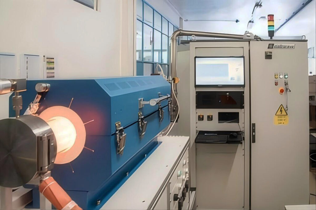
LPCVD equipment is relatively simple, consisting primarily of a reaction chamber, heating system, gas delivery system, and vacuum system, resulting in relatively low equipment costs. PECVD equipment, however, requires a plasma generator (such as an RF power source or microwave source) and a complex plasma control and monitoring system, resulting in a more complex and relatively high cost. LPCVD operating costs primarily consist of energy consumption (for heating the reaction chamber and maintaining the vacuum environment) and gas consumption. Due to the higher reaction temperature, energy consumption is relatively high. While PECVD operates at a lower temperature, the plasma generator consumes significant amounts of electricity and has higher gas purity and flow requirements, potentially leading to higher gas costs. Overall, the operating costs of the two technologies vary depending on the specific process requirements and production scale. However, in large-scale production, the difference in operating costs can have a significant impact on production costs.
Application Comparison
LPCVD Applications: LPCVD has a wide range of applications in semiconductor manufacturing, such as the deposition of insulating layers, doping layers, and metal interconnect layers in integrated circuits, as well as in the fabrication of semiconductor devices (such as transistors and diodes). In optoelectronics, it is used to form high-quality optical thin films (such as antireflection coatings and reflective films) and key structures in optoelectronic devices (such as laser diodes and light-emitting diodes). In MEMS, it is used to fabricate high-precision microstructures (such as cantilevers and microgears) and sensors (such as pressure sensors and accelerometers).
PECVD Applications: PECVD’s low-temperature deposition characteristics give it advantages in the fabrication of temperature-sensitive materials and devices, such as thin-film deposition on substrates like plastic and glass. This is used in the manufacture of flat-panel displays (such as liquid crystal displays and organic light-emitting diode displays), as well as in flexible electronic devices (such as flexible circuit boards and wearable devices). Due to its fast deposition rate and high throughput, it is also widely used in solar cell manufacturing, such as the deposition of antireflection coatings, passivation layers, and semiconductor films in crystalline silicon solar cells and thin-film solar cells.
Conclusion
Low-pressure chemical vapor deposition (LPCVD), as an important thin-film deposition technology, plays an irreplaceable role in numerous fields, including modern materials science and semiconductor manufacturing. By utilizing thermal energy to drive chemical reactions in a low-pressure environment, LPCVD can precisely deposit a variety of high-quality thin films on substrate surfaces, offering significant advantages such as excellent film uniformity, high crystal quality, and controllable stress. LPCVD is widely used in semiconductor manufacturing, optoelectronics, microelectromechanical systems (MEMS), solar cells, and data storage. In semiconductor manufacturing, it is one of the core technologies for constructing integrated circuits and semiconductor devices, crucial for achieving high performance, high integration, and reliability in chips. In optoelectronics, optical thin films and optoelectronic devices produced using LPCVD provide critical support for the development of technologies such as optical communications, lighting, and displays. In the MEMS field, LPCVD-fabricated microstructures and sensors enable the integration of tiny mechanical components with electronic circuits, promoting the application of MEMS technology in numerous fields. In solar cells and data storage, LPCVD has also made significant contributions to improving battery efficiency and storage performance.