The Ultimate Guide to Magnetron Sputtering
Magnetron sputtering technology is like a shining star, occupying a pivotal position in materials science and thin film preparation. It can prepare high-quality and high-precision thin films on various substrate materials, providing solid technical support for breakthroughs in many cutting-edge scientific and technological fields.
- High Film Quality
- Strong Parameter Controllability
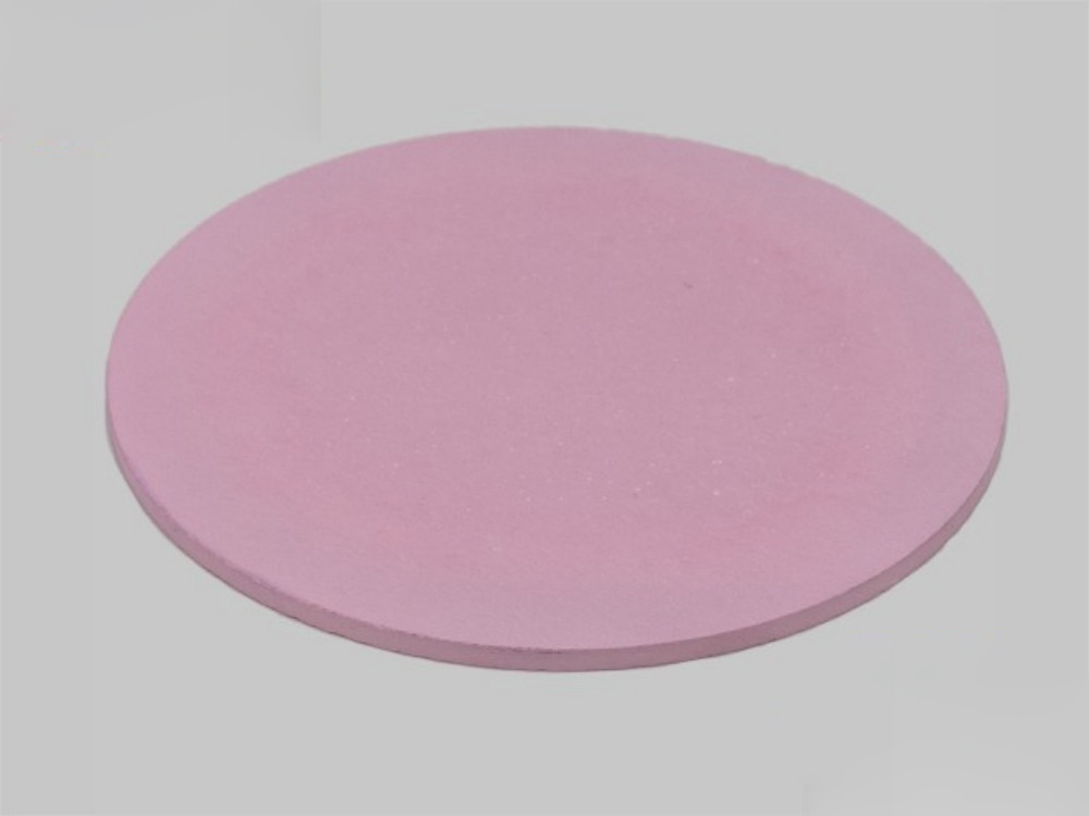
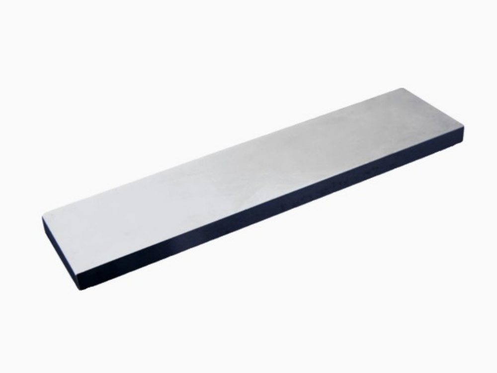
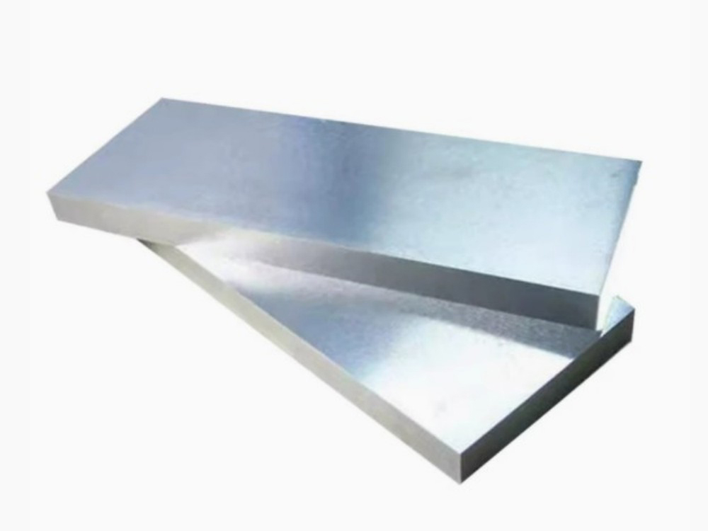
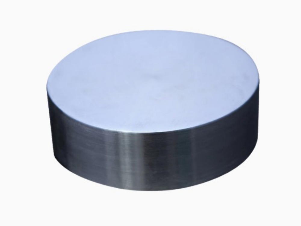
- Wide Range of Applicable Materials
- Wide Range of Applicable Materials
- Wide Range of Applicable Materials
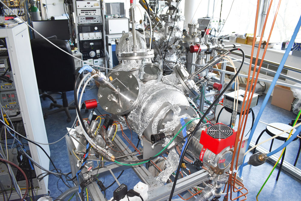
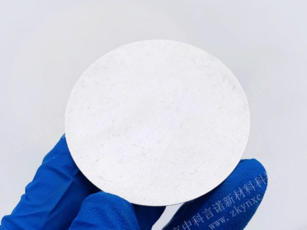
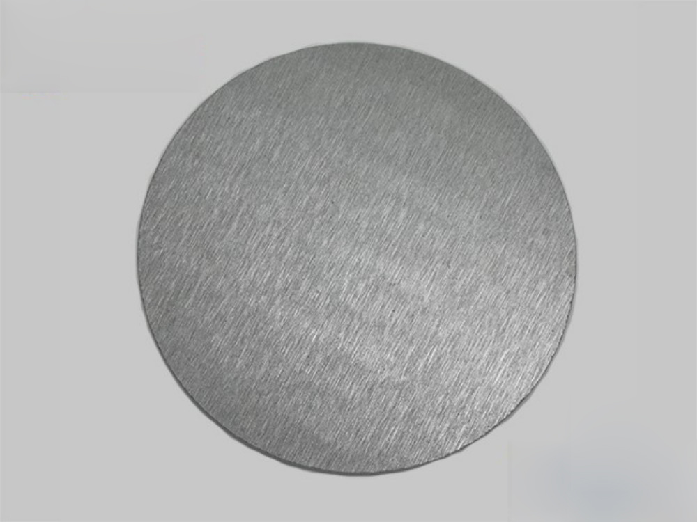
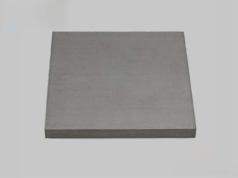
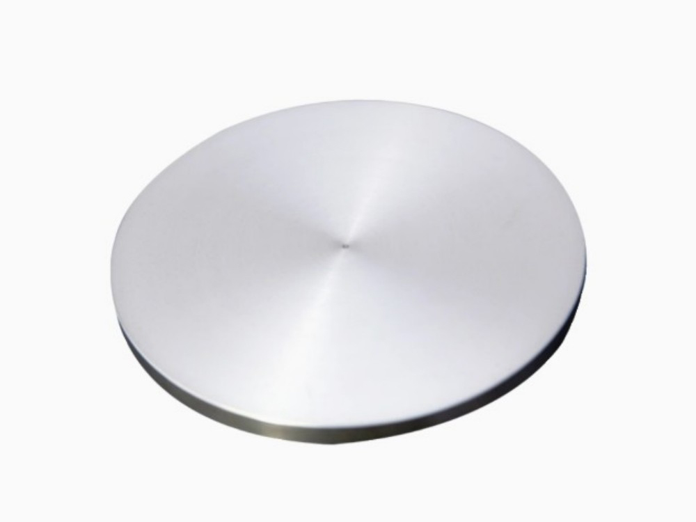
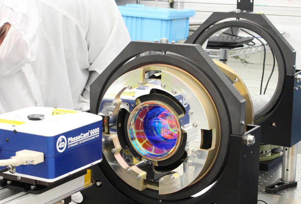
Wstitanium Workshop
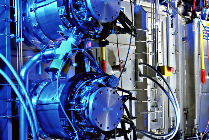
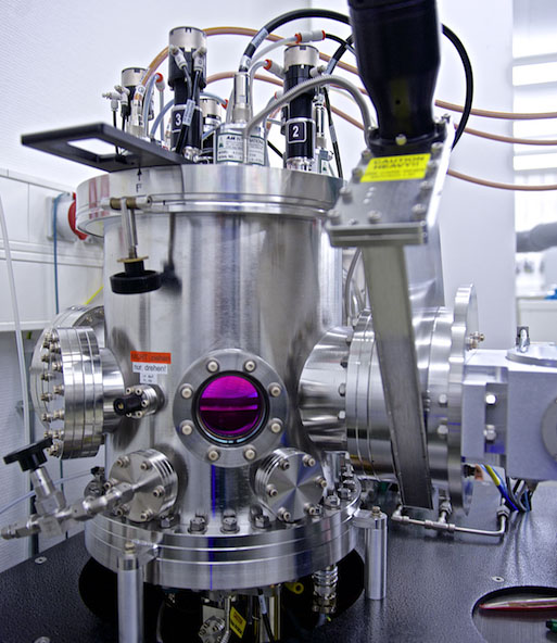
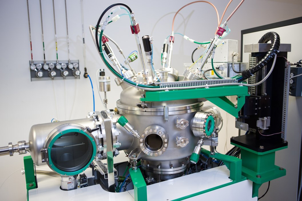
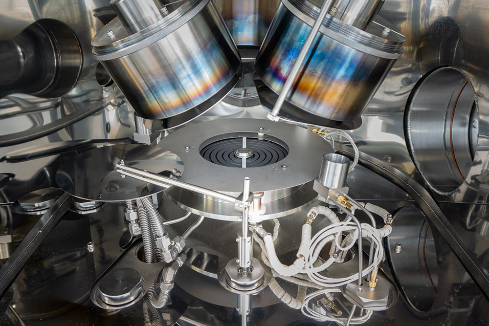
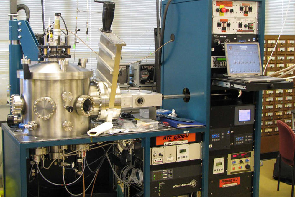
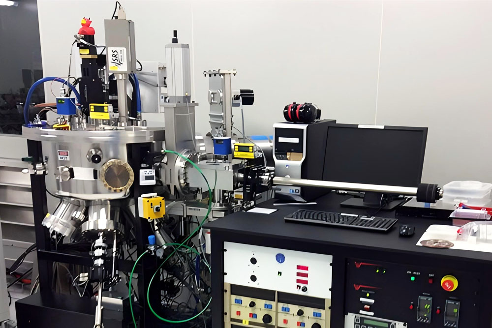
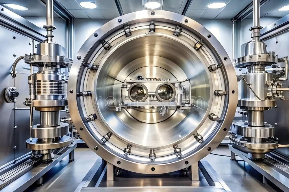
Our Powerful Facilities
Everything You Should Know About Magnetron Sputtering
Magnetron sputtering, as an advanced physical vapor deposition technology, has developed into an indispensable key technology in the field of materials science and engineering since its birth, relying on its unique advantages in thin film preparation. From the miniaturization and high performance of electronic devices, to the high precision and multifunctionality of optical components, to the high efficiency and stabilization of new energy materials. With its unique advantages, magnetron sputtering has become a key means to achieve the performance improvement of these materials.
What is magnetron sputtering?
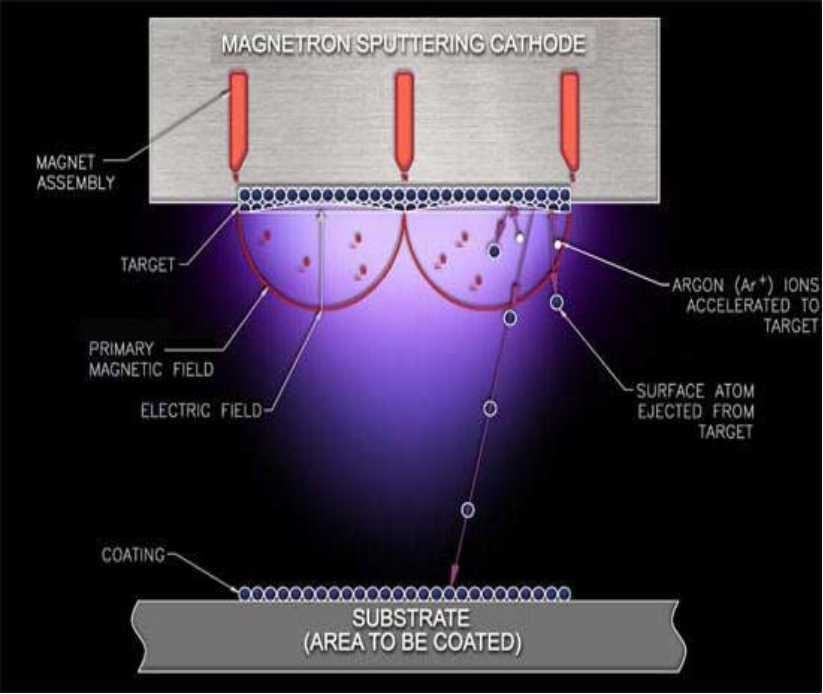
Magnetron sputtering refers to the bombardment of target or source materials with high-energy particles, causing their atoms to be ejected from the target or source material and deposited on the substrate. Further, in sputtering, the material to be deposited is used as a target, placed in a vacuum environment, and an appropriate amount of inert gas (such as argon) is introduced. Under the combined action of the electric field and the magnetic field, the inert gas is ionized into ions. These high-energy ions bombard the surface of the target material under the acceleration of the electric field, so that the target atoms gain enough energy to escape from the surface. The sputtered atoms, molecules or ions fly in the vacuum and are finally deposited on the surface of the substrate to form a uniform and dense film.
History of Magnetron Sputtering
The development of magnetron sputtering technology is a history of technological evolution full of innovation and breakthroughs. In the 1930s, the sputtering phenomenon was first discovered, opening the door to exploration in this field, but the technology was not mature at the time and there were many limitations, so it was not widely used. In the 1960s, with the growing demand for thin film preparation, sputtering technology began to receive more attention, and scientists continued to try to improve it. However, problems such as low sputtering rate and high substrate temperature of traditional sputtering technology still restricted its development. It was not until the 1970s that magnetron sputtering technology made a major breakthrough. Chapin invented a planar magnetron sputtering target suitable for industrial applications. By cleverly introducing a magnetic field, he successfully solved many problems of traditional sputtering and achieved high-speed and low-temperature sputtering, making magnetron sputtering technology have the conditions for large-scale industrial production and quickly applied in electronics, optics and other fields.
Since then, magnetron sputtering technology has continued to develop, with new technologies and applications emerging continuously, from the initial simple metal film preparation to the current ability to prepare complex multi-component compound films, nanostructured films, etc., and its application areas have also expanded from electronics and optics to new energy, biomedicine, aerospace and other fields.
Principle of Magnetron Sputtering
In a magnetron sputtering system, the movement of electrons is the key starting point of the entire sputtering process. When a DC voltage is applied between the target (cathode) and the substrate (anode), the electrons escape from the target surface under the action of the electric field force and accelerate toward the substrate. However, unlike traditional sputtering, magnetron sputtering sets a magnetic field near the target surface. According to the Lorentz force law, the moving electrons in the magnetic field will be affected by the Lorentz force, and its direction is perpendicular to the direction of the electron’s movement and the direction of the magnetic field. Under the action of this composite field, the trajectory of the electron’s movement is bent, and it is no longer a simple linear motion, but a complex spiral motion near the target surface.
During the movement, the electrons constantly collide with inert gas atoms such as argon, transfer energy to the gas atoms, ionize the gas atoms, generate a large number of electrons, ions and neutral particles, and thus form plasma.
Mode of Magnetron Sputtering
DC Magnetron Sputtering
DC magnetron sputtering is the most basic and common mode in magnetron sputtering technology. A DC power supply is directly connected to the target material, making the target material a cathode. After the system is evacuated and filled with an appropriate amount of argon gas, a DC voltage is applied between the target material and the substrate to form an electric field. Electrons escape from the surface of the target material under the action of the electric field, and make spiral motion under the constraint of the magnetic field, colliding with argon atoms to ionize them. The generated argon ions bombard the target material under the acceleration of the electric field, achieving sputtering of target atoms and deposition of thin films.
RF Magnetron Sputtering
RF magnetron sputtering is mainly used to solve the problem that DC magnetron sputtering cannot sputter insulating materials. It uses a radio frequency power supply (usually with a frequency of 13.56 MHz) instead of a DC power supply. Under the action of the radio frequency electric field, electrons and ions make high-frequency oscillation motion in the electric field. When electrons collide with argon atoms, the argon gas is ionized to produce plasma. The RF electric field neutralizes the charge on the surface of the insulating target through capacitive coupling, achieving stable sputtering of the insulating material. RF magnetron sputtering is suitable for sputtering various insulating materials, such as ceramics, oxides, nitrides, etc.
Pulsed Magnetron Sputtering
Pulsed magnetron sputtering is a new sputtering mode developed on the basis of DC magnetron sputtering. In the high voltage stage of the pulse, the plasma density increases sharply and the sputtering rate increases significantly; in the low voltage stage of the pulse, the plasma density decreases, the charge on the target surface is dissipated, and the occurrence of abnormal phenomena such as arc discharge is reduced. This sputtering mode is used in the preparation of high-performance metal films, compound films, and fields with extremely high film quality requirements, such as semiconductor devices and magnetic recording media.
Reactive Magnetron Sputtering
Magnetron reactive sputtering is an important technology for preparing compound films. In sputtering, in addition to inert gases such as argon, reactive gases such as oxygen, nitrogen, and methane are also introduced at the same time. When the target atoms are sputtered out, they react chemically with the reactive gas molecules in flight to form compounds, which are deposited on the substrate surface to obtain compound films. It has broad application prospects in the preparation of various functional films, such as optical films, semiconductor films, and superconducting films. However, the magnetron reactive sputtering process is relatively complicated.
Balanced Magnetron Sputtering
Balanced magnetron sputtering is based on the confinement of electrons by magnetic fields. Under the acceleration of the electric field, electrons collide with gas molecules (usually argon) to produce argon ions and new electrons. Argon ions bombard the surface of the target material under the action of the electric field, causing the target atoms to be sputtered out, and these sputtered atoms are then deposited on the surface of the substrate to form a thin film. Balanced magnetron sputtering has certain limitations. The bombardment of ions on the film is weak, resulting in a relatively low bonding force between the film and the substrate.
Unbalanced Magnetron Sputtering
Unbalanced magnetron sputtering is to adjust the magnetic field distribution of the magnetron sputtering target source so that the magnetic field on the surface of the target source is in an unbalanced state. The magnetic flux of the outer magnetic pole of the target source is greater than that of the inner magnetic pole, resulting in incomplete closure of the two-pole magnetic field lines on the target surface, and part of the magnetic field lines extend to the substrate area. In this way, electrons can extend to the substrate along the magnetic field lines, increasing the plasma density and gas ionization rate in the substrate area.
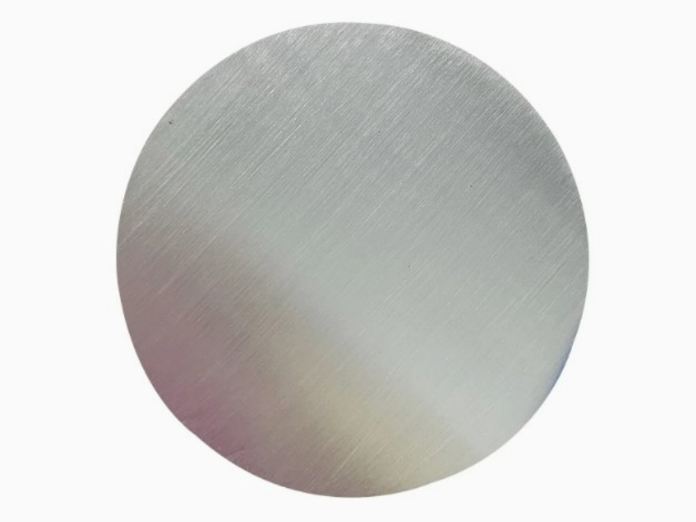
Ytterbium Sputtering Target
Ytterbium is a silvery-white metal with an atomic number of 70 and a melting point of about 824°C. Ytterbium targets are mainly used as evaporation materials for metal coatings of organic light-emitting materials (OLEDs). In the laser field, it is used for high-power fiber lasers and solid laser crystal coatings. In nuclear applications, it is used for coatings of neutron poison control rods in nuclear reactors and radiation-proof linings for spent fuel transport containers.
Bismuth Sputtering Target
The symbol for bismuth is Bi, with an atomic number of 83. It is a silvery-white metal with a light red luster and is hard and brittle. Bismuth targets are widely used in aerospace, automotive lighting, OLED and optical industries, such as fuel cells, semiconductors, displays, LEDs and photovoltaics, glass coatings and other fields. In addition, bismuth is also used in the metallurgical industry for specific alloys, using some of its properties to improve alloy performance.
Dysprosium Sputtering Target
In the field of nuclear energy safety, zinc oxide doped dysprosium oxide targets can be used for real-time monitoring coatings for neutron flux in molten salt reactors and first wall damage detection sensors for fusion reactors. In terms of deep ultraviolet devices, they can be used for day-blind ultraviolet communication photocathodes, 230-280nm band micro lasers, etc. They are also used in the field of radiation imaging, such as high-resolution neutron photography conversion screens, etc.
Erbium Sputtering Target
Erbium is a chemical element with the symbol Er, atomic number 68, silvery white metallic luster, and a melting point of 1412℃. Erbium targets also have important applications in the fields of optics and electronics, such as in the field of optical communications. Erbium ion-doped fiber amplifiers (EDFAs) are key devices that can amplify optical signals and greatly improve the transmission distance and capacity of optical communication systems.
Cobalt Sputtering Target
Cobalt is a transition metal with a high melting point (about 1495℃) and good ductility. Its common forms include discs, rectangular plates, etc., with diameters ranging from 50 mm to 200 mm, and thickness can be customized according to needs. Cobalt targets are mainly used for the preparation of magnetic films, conductive layers, and barrier layers. For example, in hard disks, cobalt-based alloy films can increase storage density.

Rhenium Sputtering Target
The density of rhenium is as high as 21.04g/cm³, and its melting point ranks third among all elements, up to 3186°C, and its boiling point ranks first, reaching 5596°C. Rhenium targets are used to prepare high-performance electronic components and integrated circuits, high-temperature sensors, and protective layers for nuclear reactors. When rhenium is alloyed with metals such as tungsten and molybdenum, its comprehensive performance is better.
Niobium Sputtering Target
Niobium is mainly used in the semiconductor and microelectronics industries, and can be used in touch screens, optical lenses, and glass coatings. Since niobium has good superconducting properties, the thin films prepared by its target can be used in superconducting material related fields, such as superconducting magnets, MRI scanners, etc.
Praseodymium Sputtering Target
Praemonium can be used to prepare thin films with special optical properties, such as optical filters, laser crystals, etc., using the specific spectral absorption of praseodymium ions to achieve selective transmission or absorption of light. Magnetic films prepared by sputtering praseodymium targets can enhance storage density and stability.
Iridium Sputtering Target
Iridium has an atomic number of 77 and is one of the metals with the highest density at room temperature. Its melting point is 2466°C. It has extremely strong corrosion resistance, is insoluble in ordinary acids, has excellent oxidation resistance, and has low resistivity. In the field of electronic semiconductors, it can be used for electrodes or seed layers of MRAM.
Antimony Sputtering Target
Antimony atomic number 51. In the field of advanced flame retardancy, antimony can be used for fireproof coatings of new energy vehicle battery packs and smoke and poison suppression layers of aviation composite materials. In optoelectronic integration, it can be used for flexible OLED packaging barrier layers and smart window electrochromic-flame retardant dual-functional layers. In the field of semiconductor packaging, it can be used for 3D IC wafer-level plastic packaging materials and high-density PCB flame retardant media.
Thulium Sputtering Target
Thulium atomic number 69. In the field of lasers, thulium ion-doped laser materials can be used to generate mid-infrared lasers, which have important applications in the medical field, such as laser surgery, because of its penetration depth and thermal effects on human tissues, it can achieve precise tissue cutting and treatment. In optical communications, thulium-related optical films can be used to regulate and process optical signals. In addition, thulium films can be used to improve the optical performance of instruments.
Rhodium Sputtering Target
Rhodium atomic number 45, silvery white, hard, corrosion-resistant, and has good chemical inertness. The hardness of rhodium target is 4~4.5, the relative density is 12.5, and the melting point is as high as 1955℃. Because of its corrosion resistance and good gloss. In the field of automobile exhaust purification, the coating prepared by rhodium target can be used as a catalyst to reduce pollutant emissions. In addition, in the production of some high-end jewelry, rhodium target electroplating is also used to enhance the beauty and durability of jewelry.
Ruthenium Sputtering Target
Ruthenium is relatively rare in nature. Ruthenium targets are important materials for manufacturing high-precision electronic components. In the semiconductor industry, it can be used to manufacture magnetic heads for hard disk drives, resistor layers for large-scale integrated circuits, and electrodes for high-definition flat-panel displays.
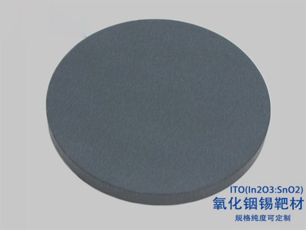
Indium Tin Oxide Sputtering Target
It is a target material made of indium oxide (In₂O₃) and tin oxide (SnO₂) in a certain proportion, usually containing about 90% indium oxide and about 10% tin oxide. It is widely used in display devices such as liquid crystal displays (LCDs), organic light-emitting diode displays (OLEDs), touch screens, as well as solar cells, transparent electrodes and other fields.
Holmium Sputtering Target
Holmium has an atomic number of 67 and a melting point of about 1474℃. In nanoscale quantum magnetic imagers, holmium ion spin probe arrays can achieve a spatial resolution of 0.5nm. In implantable nuclear medical batteries, it has the advantages of long continuous power supply time.
Advantages of Magnetron Sputtering
Excellent film quality
The thin films prepared by magnetron sputtering have the characteristics of good uniformity, high density and strong adhesion. It effectively reduces the pores and defects in the film and improves the mechanical properties and chemical stability of the film. In addition, the target atoms form a strong binding force with the atoms on the surface of the substrate during the deposition on the surface of the substrate and are not easy to fall off.
Wide range of applicable materials
Magnetron sputtering can sputter almost all metals, alloys, semiconductors, insulators and other materials, including high melting point materials and complex compound materials. For example, metals (aluminum, copper, titanium, etc.), alloy materials (titanium aluminum alloy, nickel-chromium alloy, etc.), semiconductor materials (silicon, gallium arsenide, etc.), and insulating materials (silicon dioxide, aluminum oxide, etc.).
High deposition rate
Compared with traditional sputtering technology, magnetron sputtering effectively constrains the movement of electrons by introducing a magnetic field, increases the probability of collision between electrons and gas atoms, and increases the plasma density, thereby significantly increasing the sputtering rate. High deposition rate means that a film of the required thickness can be prepared in a shorter time, which improves efficiency, reduces costs and is suitable for large-scale production.
Low substrate temperature
In magnetron sputtering, electrons are confined near the target by a magnetic field, which reduces the bombardment of the electrons on the substrate, thereby reducing the temperature rise of the substrate. This feature is very important for substrate materials that are sensitive to temperature (such as plastics, polymers, semiconductor chips, etc.), to avoid deformation, performance degradation or damage of the substrate due to high temperature.
Strong controllability
Various parameters in magnetron sputtering (such as sputtering power, gas flow and ratio, working pressure, substrate bias, sputtering time, etc.) can be precisely controlled to achieve precise control of the thickness, composition, structure and performance of the film. For example, by controlling the flow of the reaction gas, compound films of different compositions can be prepared; by adjusting the sputtering power, the growth rate of the film can be controlled.
Easy to industrialize
Magnetron sputtering equipment has the characteristics of relatively simple structure, convenient operation and good stability. According to the needs, magnetron sputtering systems of different sizes are designed, from small equipment in the laboratory to large-scale industrial production lines. At the same time, magnetron sputtering technology can prepare thin films on substrates of various shapes and sizes, including flat, curved and complex-shaped substrates.
Disadvantages of Magnetron Sputtering
Although magnetron sputtering technology has many advantages, it also has some shortcomings that need to be considered and improved in practical applications:
High equipment cost
Magnetron sputtering equipment requires multiple complex components such as vacuum system, power system, magnetic field system, etc., and its manufacturing and maintenance costs are relatively high. Especially for some special types of magnetron sputtering equipment (such as RF magnetron sputtering, pulse magnetron sputtering equipment).
Low target material utilization
In magnetron sputtering, ions mainly bombard specific areas on the surface of the target material (usually areas with strong magnetic fields), resulting in uneven corrosion of the target material and forming “etching grooves”, which makes the target material utilization rate low, generally around 30%-50%.
High film stress
There is often a certain amount of internal stress in the film prepared by magnetron sputtering, which is mainly due to the lattice distortion and defects generated during the atomic deposition process when high-energy particles bombard the substrate surface. Large internal stress may cause cracking and peeling of the film.
Complex-shaped substrates
Although magnetron sputtering can prepare thin films on substrates with complex shapes, it is difficult to ensure the uniformity of the film for some substrates with complex structures such as deep holes and grooves. Due to the linear motion characteristics of the sputtered particles, the film thickness may be thin or unable to be deposited in the shadow area of the substrate.
Some materials are difficult to sputter
Although magnetron sputtering is applicable to a wide range of materials, the sputtering process may be difficult for some materials with low vapor pressure, high melting point, or materials that easily form compounds. For example, some ceramic materials are prone to target poisoning during the sputtering process.
Potential contamination
In magnetron sputtering, especially in reactive sputtering, some harmful gases (such as ozone, nitrogen oxides, etc.) may be generated, or dust particles generated during the target sputtering process may have a certain impact on the health of operators and the environment.
Magnetron Sputtering Applications
Magnetron sputtering is widely used in many fields such as electronic information, optics, new energy, biomedicine, aerospace, decoration and protection, etc. Whether it is metal interconnects in integrated circuits, transparent electrodes in display devices, or absorption layers in solar cells, thermal protection coatings on aerospace equipment, they all rely on the support of magnetron sputtering technology.
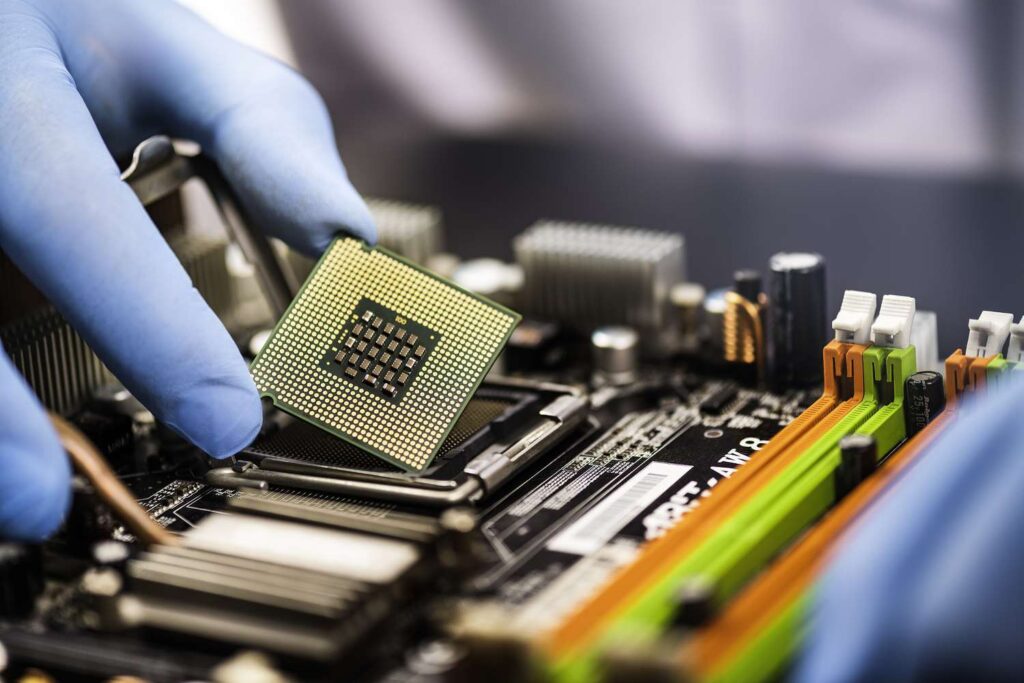
Electronics
Magnetron sputtering is used to prepare metal interconnects (such as aluminum and copper films), diffusion barriers (such as titanium nitride and tungsten films), insulating layers (such as silicon dioxide and silicon nitride films), etc. In display devices such as liquid crystal displays (LCDs) and organic light-emitting diodes (OLEDs), magnetron sputtering technology is used to prepare transparent conductive electrodes (such as indium tin oxide ITO films), metal electrodes, isolation layers, etc.
Optics
The application of magnetron sputtering technology in the field of optics is mainly reflected in the preparation of optical thin films. The preparation of anti-reflection films (such as multilayer films of alternating silicon dioxide and titanium dioxide) on the surfaces of optical lenses, eyeglasses, displays, etc. can reduce the reflection loss of light, improve the transmittance, make the image clearer and the picture brighter. It is used to manufacture reflectors (such as aluminum and silver films), laser resonator reflectors, etc. Highly reflective films can reflect most of the incident light back and play an important role in telescopes, laser equipment, etc.
New Energy
The application of magnetron sputtering technology in the field of new energy is mainly concentrated in solar cells, lithium-ion batteries, etc., providing key support for the development and utilization of new energy. In the preparation of thin-film solar cells (copper indium gallium selenide, cadmium telluride, gallium arsenide solar cells, etc.), magnetron sputtering technology is used to deposit key thin film layers such as absorption layers, window layers, and transparent electrodes. Magnetron sputtering technology can be used to prepare electrode materials and diaphragm coatings. For example, sputtering a layer of nano-metal film (such as tin or silicon film) on the surface of an electrode can improve the conductivity and lithium storage capacity of the electrode.

Biomedicine
Preparing antibacterial coatings (such as silver and copper films) on the surface of medical devices (such as scalpels, syringes, and implantable medical devices) can inhibit the growth and reproduction of microorganisms such as bacteria and fungi, reduce the risk of infection during the use of medical devices, and improve medical safety. For implantable medical devices such as artificial joints, dental implants, and cardiovascular stents, their surfaces need to have good biocompatibility to avoid causing immune rejection reactions in the human body. Preparing biocompatible coatings (such as titanium, zirconium oxide, and titanium nitride films) on the surfaces of these devices through magnetron sputtering technology can improve their surface properties and promote the adhesion and growth of tissue cells.

Aerospace
The aerospace field has extremely strict requirements on the performance of materials. The films prepared by magnetron sputtering technology can significantly improve the high temperature resistance, corrosion resistance, and wear resistance of the materials, meeting the use requirements of aerospace equipment. Preparing thermal protective coatings (such as zirconium oxide, silicon carbide, and silicon nitride films) on the surface of spacecraft shells and engine components (such as turbine blades and combustion chambers) can effectively block high temperatures and protect components from being burned in extreme high temperature environments (such as when the spacecraft returns to the atmosphere or when the engine is working), thereby ensuring the safe operation of the equipment.

Conclusion
From its basic principle, magnetron sputtering technology can effectively constrain the movement of electrons and improve the plasma density through the synergistic effect of electric and magnetic fields, so as to efficiently prepare high-quality thin films. Almost all types of materials can be processed, including metals, alloys, semiconductors, insulators and complex compounds, which makes it widely used in many fields such as electronic information, optics, new energy, biomedicine, aerospace, decoration and protection. Magnetron sputtering technology has made great achievements in the past few decades. In the future development of science and technology, it will continue to play an important role and make greater contributions to the research and development and application of new materials and the technological progress of various industries.
1. http://www.semicore.com/what-is-sputtering
2. https://www.intechopen.com/online-first/63559
3.https://en.wikipedia.org/wiki/Sputter_deposition