Physical Vapor Deposition
Physical vapor deposition (PVD) is an advanced technology that uses physical means to vaporize materials into atoms, molecules or ions in a vacuum environment and deposit them on the surface of a substrate to form a thin film.
- Vacuum Ion Coating
- Vacuum Sputtering Coating
- Vacuum Evaporation Coating
- 2000+ Target Materials Options
- Films From 5 Nanometers to 50 Microns
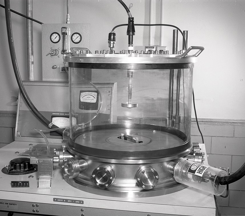
Wstitanium Workshop
Our Powerful Facilities
The Ultimate Guide to Physical Vapor Deposition
In the field of modern materials science and surface engineering, physical vapor deposition (PVD) technology occupies a pivotal position. From electronic products, precision optical instruments to key components in high-end fields such as aerospace, PVD technology is everywhere. It can deposit a layer of thin film with special functions on the surface of the material. These films can not only improve the physical properties of the material such as wear resistance, corrosion resistance, and conductivity, but also give the material unique optical, electrical and magnetic properties, greatly expanding the application range of the material. With the rapid development of science and technology, the requirements for material performance are becoming increasingly stringent. PVD technology is also constantly innovating and evolving, providing strong technical support to meet the needs of various industries.
Brief History
The origin of physical vapor deposition technology can be traced back to the early 20th century. At that time, it had some preliminary applications, but due to technical conditions, it developed slowly. The real rapid development began in the past 30 years. With the continuous progress of vacuum technology, plasma technology and material science, PVD technology has gradually matured and has been widely used in many fields.
In the 1960s, ion plating technology was proposed by D.M.Mattox, laying an important foundation for the development of PVD technology. Thereafter, in the 1970s, Bunshah and Juntz introduced reactive evaporation ion plating (AREIP), successfully depositing superhard films such as TiN and TiC. These superhard films have extremely high hardness and wear resistance, greatly expanding the application of PVD technology in the industrial field, such as tool coating. At the same time, Moley and Smith developed and perfected hollow hot cathode ion plating, and in 1973 developed radio frequency ion plating (RFIP), further enriching the means and application scope of PVD technology.
In the 1980s, magnetron sputtering ion plating (MSIP) and multi-arc ion plating (MAIP) came out one after another. Magnetron sputtering ion plating combines the advantages of magnetron sputtering and ion plating, improving the deposition rate and film quality; multi-arc ion plating has emerged in the field of surface treatment with its high ionization rate and high deposition rate, and is widely used in the preparation of surface coatings for molds, mechanical parts, etc.
Entering the 1990s, PVD technology has been increasingly widely used in the watch industry, especially in the surface treatment of high-end watch metal appearance parts. Its exquisite coating effect and good wear resistance add unique charm and value to watches. With the continuous innovation of PVD technology, a series of advanced technologies have emerged, including multi-arc ion plating and magnetron sputtering compatible technology, large rectangular long arc targets and sputtering targets, unbalanced magnetron sputtering targets, twin targets, strip foam multi-arc deposition winding coating, strip fiber fabric winding coating, etc. The coating equipment used is also developing towards computer full automation and large-scale industrial scale. This makes it play an indispensable role in many fields such as aerospace, electronics, optics, machinery, construction, light industry, metallurgy, etc.
PVD Working Principle
Physical vapor deposition (PVD) refers to the technology of vaporizing the surface of the material source (solid or liquid) into gaseous atoms, molecules or partially ionized into ions under vacuum conditions by physical methods, and depositing a thin film with certain special functions on the surface of the substrate through low-pressure gas (or plasma). Its basic principle can be divided into three key steps:
Vaporization
The plating material is evaporated, sublimated or sputtered by heating, sputtering, arcing, etc., so as to form a vaporization source of the plating material. For example, in vacuum evaporation coating, the solid plating material is heated to the evaporation temperature by resistance heating, electron beam heating, etc., so that it is converted into gaseous atoms or molecules; in sputtering coating, high-energy ions are used to bombard the target material so that the atoms on its surface obtain enough energy to escape and form gaseous atoms or molecules.
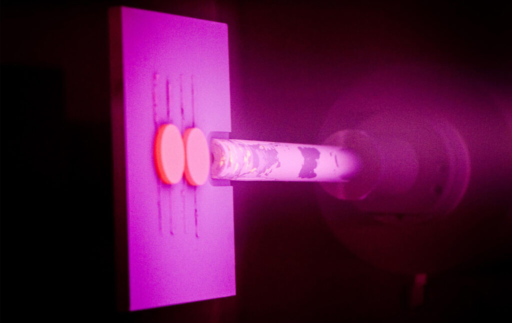
Migration
The vaporized plating atoms, molecules or ions migrate in a vacuum environment or low-pressure gas or plasma. During the migration process, they will collide with other particles, resulting in various reactions such as scattering and excitation. For example, in a plasma environment, ions will accelerate under the action of the electric field, collide with gas molecules and ionize them, further increasing the density and activity of the plasma.
Deposition
The plating atoms, molecules or ions that migrate to the surface of the substrate are adsorbed, diffused, nucleated and grown on the surface of the substrate, and finally form a continuous film. During deposition, atoms or ions will find a suitable position on the surface of the substrate to attach, and gradually gather to form tiny crystal nuclei. With the arrival of more atoms or ions, the crystal nuclei continue to grow and connect with each other, and finally form a complete film.
Types of PVD
PVD technology is mainly divided into three categories: vacuum evaporation coating, vacuum sputtering coating and vacuum ion coating. Let’s compare the three PVD technologies in a table:
| Type | Sub – Classification | Principle |
| Vacuum Evaporation Coating | Resistance Heating Evaporation Coating | When an electric current passes through a resistor, heat is generated. The heat makes the coating material evaporate. The evaporated material condenses on the substrate surface to form a film. For example, when preparing a metal film, place the metal or metal sheet on a resistance – heated evaporation source (such as a tungsten filament). After electrification, the heating element generates heat to make the metal material evaporate and coat. |
| Electron Beam Evaporation Coating | Use a high – energy electron beam to bombard the coating material. The kinetic energy of electrons is converted into thermal energy to make the coating material evaporate. The electron beam is generated by an electron gun. Evaporate the coating material in a high – vacuum environment to achieve high – point evaporation of the material. It is often used to prepare optical thin films, semiconductor thin films, etc., such as evaporating titanium dioxide (\(TiO_2\)) to prepare optical anti – reflection films. | |
| Arc Discharge Evaporation Coating | Generate an arc between the cathode and anode to make the coating material evaporate and ionize. The high temperature of the arc can make the coating material evaporate and ionize rapidly. The ions are accelerated by the electric field and deposited on the substrate surface. For example, when preparing a hard alloy coating, use arc discharge to evaporate metal compounds, and deposit a hard coating on the tool surface. | |
| Laser Beam Evaporation Coating | Use a high – energy – density laser beam to irradiate the coating material, so that the coating material is evaporated and ionized simultaneously. The high energy of the laser can precisely control the evaporation area and evaporation amount, and is suitable for preparing special thin films and micro – nano structure films. For example, when preparing an ultra – hard film on a tool, select appropriate materials and make the laser ablation meet the design requirements. | |
| Vacuum Sputtering Coating | DC Sputtering Coating | In a vacuum environment, introduce an inert gas (such as argon). Use a DC voltage to make the gas generate plasma between the electrodes. Positive ions are accelerated by the electric field to bombard the target material, and the sputtered target atoms are deposited on the substrate surface to form a film. It is often used for the deposition of metal films, such as sputtering a metal film on glass to prepare a metal – coated glass for reflection. |
| RF Sputtering Coating | For insulating materials, use an RF power supply to generate an RF electric field to make the gas plasma. The RF electric field can make electrons oscillate in the electric field, collide with gas molecules to ionize, and generate plasma, so as to realize the sputtering coating of insulating materials. It can be used to prepare oxide, nitride and other insulating films, such as sputtering a silicon dioxide (\(SiO_2\)) film for the insulation of integrated circuits. | |
| Magnetron Sputtering Coating | Introduce a magnetic field in the sputtering chamber. Under the action of the magnetic field, the movement path of electrons is extended, increasing the collision probability between electrons and gas molecules, improving the ionization rate of the gas and the utilization rate of the target. It is widely used in the preparation of various thin films, such as sputtering a transparent and conductive indium tin oxide (ITO) film on a flat panel display. | |
| Vacuum Ion Coating | Ion Coating | Make the coating material evaporate, sputter or be generated by other means in an electric field to ionize the coating material. Under the action of the electric field on the substrate, the ions are accelerated and deposited on the substrate to form a film. The film – substrate bonding force of ion coating is strong, and the film layer is dense and uniform, and can be used for the surface coating of various materials, such as coating a titanium nitride (TiN) film on a mold surface to improve wear resistance. |
| Reactive Ion Coating | During the ion coating process, introduce a reactive gas (such as oxygen, nitrogen, etc.), which reacts with the evaporated coating material atoms on the substrate surface to form a compound film. For example, introduce oxygen, and the evaporated titanium ions react with oxygen to form a titanium dioxide (\(TiO_2\)) film on the substrate surface, which can be used for optics, photocatalysis and other fields. | |
| Multi – arc Ion Coating | Use cathode arc discharge to generate multiple arc spots on the target surface. The coating material at the arc spots is evaporated and ionized simultaneously. The ions are accelerated and deposited on the substrate surface under the action of the electric field. The ionization rate of the coating material of multi – arc ion coating is high, and the deposition rate is fast. It is often used to prepare decorative and functional coatings, such as coating a gold film on hardware surfaces for decoration. |
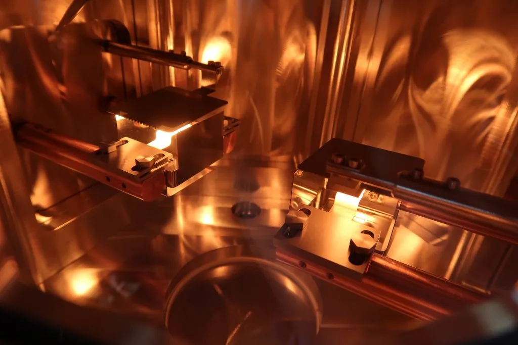
PVD Operation Steps
Material preparation: Select appropriate plating materials and substrate materials. Plating materials should be selected according to the performance and application of the required film. For example, if you want to prepare a wear-resistant coating, you can choose TiN, CrN and other materials; the substrate material should consider its compatibility with the film and the application scenario, such as metal substrates are often used for mechanical parts coating. Glass substrates are often used for optical films. Ensure the purity and quality of the plating material and substrate materials, remove impurities, oil stains and oxides on the surface, and use chemical cleaning, ultrasonic cleaning and other pretreatments. For some applications with extremely high surface quality requirements, polishing may also be required.

Equipment preparation: Check and debug PVD equipment, including vacuum system, heating system, power system, gas supply system, etc. Ensure that the vacuum system can reach the required vacuum degree. Generally, PVD needs to be carried out in a high vacuum environment, and the vacuum degree is usually required to reach 10⁻³ – 10⁻⁶ Pa or even lower. The heating system must be able to accurately control the temperature to meet the requirements of plating gasification. The power system must be stable and reliable, providing appropriate voltage and current for various ionization and sputtering processes. The gas supply system must ensure the purity and flow of the gas. Depending on different PVD methods and thin film materials, argon, nitrogen, oxygen and other gases may need to be introduced.

Furnace loading: Install the pre-treated substrate and plating material into the vacuum chamber of the PVD equipment. The substrate should be placed in a suitable position to ensure that it can evenly receive the deposition of the plating material. A special fixture or hanger can be used to fix the substrate. The plating material is installed in the evaporation source, target material and other positions. For example, in resistance evaporation coating, the plating material is placed on the resistance heating element; in sputtering coating, the target material is installed on the sputtering cathode. During the installation process, care should be taken to avoid introducing new impurities and contamination.

Vacuuming: Start the vacuum system and extract the air in the vacuum chamber to achieve the required vacuum degree. Generally, a mechanical pump is used for rough pumping to reduce the vacuum degree to about 1-10 Pa, and then a diffusion pump, molecular pump, etc. are used for high pumping to further reduce the vacuum degree to the target value. During the vacuuming process, the changes in the vacuum degree should be monitored to ensure the normal operation of the vacuum system. If there are problems such as air leakage, they should be promptly checked and resolved.

Heating and vaporization: According to the selected PVD method, the plating material is heated to vaporize. In vacuum evaporation coating, the plating material is heated and evaporated by means of resistance heating, electron beam heating, etc.; in sputtering coating, the target material is bombarded with ions in the plasma to sputter out the target atoms; in ion plating, the plating material is evaporated and ionized by means of arc discharge, etc. During the heating and vaporization process, parameters such as temperature and power must be precisely controlled to ensure the stability of the vaporization rate and quality of the plating material.

Deposition: Gaseous plating material atoms, molecules or ions migrate to the surface of the substrate in a vacuum environment and deposit on the substrate surface to form a thin film. During the deposition process, the substrate can be heated or cooled as needed to control the growth rate and quality of the film. For example, appropriately increasing the substrate temperature can promote the diffusion of atoms on the substrate surface and make the film denser; while lowering the substrate temperature may lead to increased stress in the film. At the same time, the structure and properties of the film can also be adjusted by controlling parameters such as the energy and incident angle of the ions.

Cooling and unloading: After the deposition is completed, stop heating and let the temperature in the vacuum chamber gradually decrease. After the temperature drops to a suitable range, open the vacuum chamber and remove the substrate coated with the film. During the cooling process, care should be taken to avoid problems such as cracks or peeling of the film due to rapid temperature changes. The removed samples can be subsequently tested and processed, such as film thickness measurement, composition analysis, performance testing, etc.

PVD Technology Materials

Evaporation coating requires the coating material to have a lower melting point and vapor pressure. Therefore, metals (such as aluminum, copper, gold, etc.) and some low-melting-point alloy materials (such as tin-lead alloy) are more suitable for evaporation coating. Accurately control the temperature and evaporation rate of the evaporation source to ensure the uniformity and quality of the film layer.

Sputtering coating has relatively lenient requirements on the coating material, and metals, alloys, ceramics, semiconductors, etc. are all acceptable. The sputtering rate and sputtering characteristics of different materials are different. It is necessary to select appropriate sputtering parameters according to the properties of the material, such as sputtering gas type, sputtering power, sputtering gas pressure, etc.

Ion plating combines the advantages of evaporation coating and sputtering coating to improve the bonding strength between the film layer and the substrate and the quality of the film layer. In ion plating, the coating particles are ionized and accelerated, so the coating material is required to have good conductivity or be ionized under certain conditions.
Metals
Aluminum (Al), titanium (Ti), chromium (Cr), nickel (Ni), copper (Cu), gold (Au), silver (Ag), etc. Aluminum film has good conductivity and reflectivity, and is often used in electrodes and optical reflectors of electronic devices; titanium film has excellent corrosion resistance and biocompatibility, and is widely used in medical devices, aerospace and other fields; chromium film has high hardness and good wear resistance, and is often used for surface coating of mechanical parts; gold and silver films are favored in the fields of electronics and decoration due to their good conductivity and chemical stability.

Alloy
Such as titanium aluminum alloy (TiAl), nickel chromium alloy (NiCr), etc. Alloy film can combine the advantages of multiple metals. For example, TiAl alloy film has the characteristics of both titanium and aluminum, with high high temperature strength, low density, good oxidation resistance, etc., suitable for coating of high temperature parts such as aircraft engines; NiCr alloy film has good heat resistance and corrosion resistance, and is often used in heating elements and anti-corrosion coatings.

Compounds
Carbides: such as titanium carbide (TiC), chromium carbide (CrC), etc. Carbide films have extremely high hardness, excellent wear resistance and high temperature resistance, and are often used for surface coatings of tools, molds, etc.
Nitrides: such as titanium nitride (TiN), chromium nitride (CrN), titanium aluminum nitride (TiAlN), etc. Nitride films are not only hard, but also have good chemical stability and decorative properties. TiN films are golden yellow and are often used for imitation gold decorative coatings. They are also a common material for tool coatings; TiAlN films can still maintain high hardness and oxidation resistance at high temperatures, and are suitable for high-speed cutting tools.

Oxides: such as titanium dioxide (Compounds sputtering targets), zinc oxide (ZnO), indium tin oxide (ITO), etc. TiO₂ film has photocatalytic activity, optical transmittance and corrosion resistance, and is used for photocatalytic decomposition of pollutants, solar cells and optical devices; ZnO film has piezoelectricity, semiconductor properties and UV shielding properties, and is used in sensors, electronic devices and sunscreen materials; ITO film is a transparent conductive film, widely used in electronic devices such as liquid crystal displays and touch screens.
Boride: such as titanium boride (TiB₂), zirconium boride (ZrB₂), etc. Boride films have high hardness, high melting point and good conductivity, and are used for wear-resistant coatings, electrode materials, etc.

Advantages of PVD Coating
Good performance
PVD coating has excellent properties such as high hardness, high wear resistance, and low friction coefficient. For example, the hardness of TiN coating can reach 2000-2500HV, which is 3-4 times the hardness of high-speed steel.
Strong bonding with the substrate
When the plating atoms or ions are deposited on the substrate surface, they will diffuse and chemically bond with the substrate atoms to form a strong bond. This ensures the long-term effectiveness and stability of the coating.
Multiple material options
A variety of materials such as metals, alloys, and compounds are used as plating materials to prepare films with different chemical compositions and properties. Precisely control the composition, structure, and properties of the film to meet the diverse needs of different fields.
Uniform and controllable coating thickness
PVD technology can achieve uniform coating deposition on the surface of complex-shaped substrates. Accurately calculate deposition time, power, gas flow, etc. to accurately control the thickness of the coating. From a few nanometers to tens of microns.
No pollution
Compared with traditional electroplating, PVD technology is carried out in a vacuum environment, does not use a large amount of chemical solutions, avoids the generation of wastewater, waste gas and waste residue, etc., and is environmentally friendly.
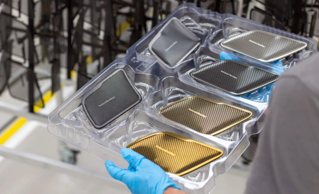
Good decorative effect
PVD coating can present a variety of colors and luster, such as gold, silver, black, rose gold, etc., and the color is long-lasting and stable, and not easy to fade. Improve the appearance quality and decorative effect of jewelry, watches, etc.
Application
PVD technology covers almost every aspect of modern industry, from electronics, optics, machinery to decoration, medical, aerospace and other fields, playing an indispensable role. It not only improves the performance and quality of parts, but also meets people’s needs for beauty, environmental protection and other aspects.
Mechanical Manufacturing
PVD coating is mainly used to improve the performance of tools, molds and mechanical parts. Tools usually choose TiN, TiCN, TiAlN and other coatings to improve the hardness, wear resistance and cutting performance of tools; the mold surface is often plated with Cr, TiAl alloy and other coatings to reduce the friction coefficient between the mold and the workpiece; for mechanical parts, such as bearings and gears, DLC (diamond-like carbon) coating can be used to reduce friction loss and improve the movement accuracy and reliability of parts.

Electronics Field
PVD coating technology is widely used in integrated circuit manufacturing, flat panel displays, sensors, etc. In integrated circuit manufacturing, high-purity metal materials (such as copper and aluminum) and semiconductor materials (such as silicon) are required for coating to prepare electrodes, interconnects and semiconductor devices; in the field of flat panel displays, ITO films are widely used as transparent conductive electrodes in LCD, OLED and other display devices; in the field of sensors, by coating films with specific functions (such as gas sensitive films, humidity sensitive films, etc.), sensors can detect specific physical or chemical quantities.

Optical Field
In the optical field, PVD coating is mainly used to prepare optical thin films, such as reflective films, anti-reflective films, filter films, etc. According to different optical performance requirements, choose appropriate optical materials and coating technology. For example, in optical instruments such as telescopes and microscopes, it is necessary to coat multiple layers of anti-reflective films to reduce the reflection loss of light on the lens surface and improve the light transmittance and imaging quality of the instrument; in laser devices, it is necessary to coat high-reflectivity reflective films to improve the output power and stability of the laser.

Aerospace
In the field of aerospace, PVD coating technology is mainly used to improve the performance of aircraft engine parts and aircraft surfaces. For example, coating TiAl alloy films on the surface of aircraft engine turbine blades can improve the high-temperature strength, oxidation resistance and thermal corrosion resistance of the blades; coating anti-radiation films on the surface of aircraft can effectively block cosmic rays and solar radiation, and protect the safety of equipment and personnel inside the aircraft.

Decoration
In the field of decoration, PVD coating is mainly used to give products beautiful appearance and good corrosion resistance. Common decorative coating materials include TiN, ZrN, CrN, gold, etc. TiN and ZrN coatings can present a golden appearance and are often used in products such as watches, eyeglass frames, and jewelry; CrN coatings can present a black appearance and are often used in products such as car wheels and bathroom hardware; gold plating can give products a luxurious golden appearance and is often used in the field of high-end decoration.

PVD vs. CVD
Physical vapor deposition (PVD) and chemical vapor deposition (CVD) are two important thin film preparation technologies. They have certain differences in principles, process characteristics, and application fields. The following is a detailed comparison of PVD and CVD in table form:
| Comparison Items | PVD (Sputtering, Thermal Evaporation, Electron Beam Evaporation, Pulsed Laser Deposition, Cathodic Arc Deposition, Magnetron Sputtering). | CVD (Chemical Vapor Deposition, Taking Common Thermal CVD and Plasma – Enhanced CVD as Examples). |
| Principle | Make the coating material gasify through physical methods, such as heating evaporation, ion sputtering, etc. Then the gaseous coating material deposits on the substrate surface to form a film. | Use gaseous chemical substances to undergo chemical reactions under conditions such as high temperature or plasma to generate solid substances and deposit them on the substrate surface to form a film. |
| Deposition Temperature | Generally relatively low, mostly below 500°C. Some processes, such as electron beam evaporation, can be carried out at room temperature. | Usually relatively high. Thermal CVD is generally between 800 – 1200°C. Plasma – enhanced CVD can be reduced to 300 – 800掳C, but it is still relatively high. |
| Thin Film Quality | The film layer is dense, has strong adhesion to the substrate, high surface finish, and low impurity content. | The film layer is relatively thick, has good crystallinity and uniform structure, but may contain a small amount of impurities, and the surface finish is relatively low. |
| Deposition Rate | Relatively low, especially for methods such as sputtering. The deposition rate is generally from several nanometers per second to dozens of nanometers per second. Thermal evaporation and electron beam evaporation are relatively faster. | Relatively high. The deposition rate of thermal CVD can reach dozens of nanometers per second to several micrometers per second. The deposition rate of plasma – enhanced CVD is also relatively fast. |
| Equipment Cost | The equipment is complex and the price is relatively high, involving multiple precision components such as vacuum systems and power supply systems. | The equipment is relatively simple, but high – temperature heating equipment and gas supply systems are required. The overall cost is also relatively high, and the maintenance cost of high – temperature equipment is relatively high. |
| Process Complexity | There are many process parameters, and high requirements for the control of vacuum degree, temperature, power, etc. The operation difficulty is relatively large. | The process involves chemical reactions, and precise control of parameters such as the flow rate, proportion, and temperature of the reaction gas is required. High requirements for the monitoring and control of the reaction process. |
| Influence on Substrate | Low – temperature deposition has little thermal influence on the substrate, and it is not easy to cause deformation and performance changes of the substrate. However, high – energy ion bombardment may cause certain damage to the substrate surface. | High – temperature deposition may cause changes in the structure and performance of the substrate material, such as causing grain growth and thermal stress of the substrate. There are certain requirements for the material and structure of the substrate. |
| Applicable Materials | Suitable for the coating of various materials such as metals, alloys, and ceramics. It can prepare metal thin films, compound thin films, etc. | Suitable for various substrate materials. It can prepare various thin films such as ceramics, semiconductors, and metals. It is especially suitable for preparing thin films of high – melting – point materials and thin films with complex structures. |
| Application Fields | Widely used in fields such as electronics, optics, machinery, and decoration, such as metal wiring in chip manufacturing, anti – reflection films for optical lenses, wear – resistant coatings for cutters, decorative coatings for watches, etc | Mainly used in semiconductor manufacturing (such as the preparation of insulating layers and diffusion layers in integrated circuits), hard alloy cutter coatings, optical fields (such as the preparation of optical fiber preforms), etc. for fields with high requirements for thin film quality and structure. |
PVD vs. Electroplating
PVD and electroplating are both common surface treatment technologies. They have obvious differences in principles, process characteristics, performance, etc. The following is a comparison in table form:
| Comparison Items | PVD (Sputtering, Thermal Evaporation, Electron Beam Evaporation, Pulsed Laser Deposition, Cathodic Arc Deposition, Magnetron Sputtering). | CVD (Chemical Vapor Deposition, taking common Thermal CVD and Plasma – Enhanced CVD as examples). |
| Principle | Gasify the coating material through physical methods, such as thermal evaporation, ion sputtering, etc. Then, the gaseous coating material deposits on the substrate surface to form a film. | Utilize gaseous chemical substances to undergo chemical reactions under conditions like high temperature or plasma to generate solid substances, which then deposit on the substrate surface to form a film. |
| Deposition Temperature | Generally relatively low, mostly below 500掳C. Some processes, such as electron beam evaporation, can be carried out at room temperature. | Usually relatively high. Thermal CVD is generally in the range of 800 – 1200°C. Plasma – Enhanced CVD can be reduced to 300 – 800°C, but it is still relatively high. |
| Thin Film Quality | The film layer is dense, has strong bonding force with the substrate, high surface finish, and low impurity content. | The film layer is relatively thick, has good crystallinity and uniform structure, but may contain a small amount of impurities, and the surface finish is relatively low. |
| Deposition Rate | Relatively low. Especially for methods like sputtering, the deposition rate is generally from several nanometers per second to dozens of nanometers per second. Thermal evaporation and electron beam evaporation are relatively faster. | Relatively high. The deposition rate of Thermal CVD can reach dozens of nanometers per second to several micrometers per second. The deposition rate of Plasma – Enhanced CVD is also relatively fast. |
| Equipment Cost | The equipment is complex and relatively expensive, involving multiple precision components such as vacuum systems and power supply systems. | The equipment is relatively simple, but high – temperature heating equipment and gas supply systems are required. The overall cost is also relatively high, and the maintenance cost of high – temperature equipment is relatively high. |
| Process Complexity | There are many process parameters, and high requirements for the control of vacuum degree, temperature, power, etc., and the operation difficulty is relatively large. | The process involves chemical reactions, requiring precise control of parameters such as the flow rate, proportion, and temperature of the reaction gas, and high requirements for the monitoring and control of the reaction process. |
| Influence on Substrate | Low – temperature deposition has little thermal influence on the substrate, and it is not easy to cause deformation and performance changes of the substrate. However, high – energy ion bombardment may cause certain damage to the substrate surface. | High – temperature deposition may cause changes in the structure and performance of the substrate material, such as causing grain growth and thermal stress of the substrate, and there are certain requirements for the material and structure of the substrate. |
| Applicable Materials | Suitable for the coating of various materials such as metals, alloys, and ceramics, and can prepare metal thin films, compound thin films, etc. | Suitable for various substrate materials, and can prepare various thin films such as ceramics, semiconductors, and metals. It is especially suitable for preparing thin films of high – melting – point materials and thin films with complex structures. |
| Application Fields | Widely used in fields such as electronics, optics, machinery, and decoration, such as metal wiring in chip manufacturing, anti – reflection films for optical lenses, wear – resistant coatings for cutters, decorative coatings for watches, etc. | Mainly used in semiconductor manufacturing (such as the preparation of insulating layers and diffusion layers in integrated circuits), hard alloy cutter coatings, optical fields (such as the preparation of optical fiber preforms), etc., for fields with high requirements for thin film quality and structure. |
Conclusion
As one of the key technologies in the field of modern material surface treatment, physical vapor deposition (PVD) technology has unique advantages and broad application prospects. PVD technology includes many types, such as vacuum evaporation coating, vacuum sputtering coating and vacuum ion coating. Each type has its own characteristics and scope of application, providing a variety of choices for different materials and application scenarios. At the same time, PVD technology has a rich selection of materials, including metals, alloys, compounds, etc., and can produce films that meet various performance requirements, such as wear-resistant, corrosion-resistant, optical, electrical and other functional films.
In the application field, PVD technology covers almost all aspects of modern industry, from high-tech fields such as electronics, optics, and machinery to daily and high-end application fields such as decoration, medical treatment, and aerospace. It plays an indispensable role. Compared with other surface treatment technologies such as chemical vapor deposition (CVD) and electroplating, PVD technology has obvious differences in principles, process characteristics, film properties, etc., and each is suitable for different application scenarios.