The Ultimate Guide to Plasma Enhanced Chemical Vapor Deposition
Plasma-Enhanced Chemical Vapor Deposition (PECVD) utilizes the unique properties of plasma to deposit high-quality thin films at relatively low temperatures, providing support for the development of numerous high-tech industries.
- Good Film Uniformity
- Higher Film Deposition Rate
- Strong Film-Substrate Bonding
- Compatible With Conductive Materials
Everything You Should Know About PECVD
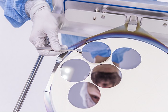
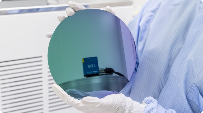
Plasma-enhanced chemical vapor deposition (PECVD) technology provides critical thin-film deposition solutions for numerous cutting-edge fields. From microelectronics and optical components to solar cells and biomedicine, PECVD is ubiquitous, driving these fields forward. This article provides a comprehensive and in-depth introduction to PECVD technology, covering its definition, principles, processes, types, typical thin films produced, advantages, and extensive applications, allowing you to appreciate both the allure and mysteries of this technology.
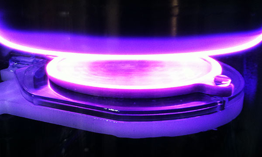
PECVD is a key variant of chemical vapor deposition (CVD). Chemical vapor deposition (CVD) involves the use of gaseous chemicals to react on a solid surface, producing a solid deposit. PECVD uses plasma to enhance the chemical reaction process. Plasmas are typically generated by radio frequency, direct current, or microwave discharges. These glow discharges excite reactant gases (such as silane or oxygen) to form a plasma. Highly reactive species such as ions, free electrons, free radicals, excited atoms, and molecules facilitate more efficient chemical reactions on the substrate surface. This results in the formation of a thin film composed of metals, oxides, nitrides, and/or polymers (fluorocarbons, hydrocarbons, silicones) on the substrate surface.
PECVD Principle
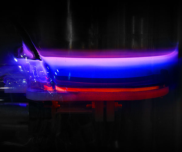
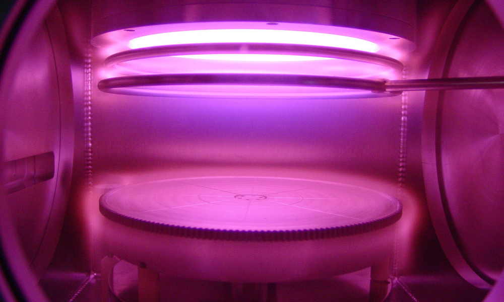
In PECVD systems, plasma is typically generated using radio frequency (RF) or microwave (MW) power. Taking RF plasma as an example, when an RF voltage is applied to electrodes within the reaction chamber, gas molecules are accelerated by the electric field and collide with other gas molecules. As these collisions continue, the gas molecules gain sufficient energy to ionize, generating electrons and ions, thus forming a plasma. This plasma is highly reactive, containing a large number of high-energy electrons, ions, and free radicals.
The high-energy electrons in the plasma collide with the reactant gas molecules, breaking their chemical bonds and generating highly reactive free radicals. These free radicals are highly reactive and can react at relatively low temperatures. For example, when the reactant gases are silane (SiH₄) and ammonia (NH₃), in the presence of the plasma, silane decomposes into silicon radicals (Si·) and hydrogen radicals (H·), while ammonia decomposes into nitrogen radicals (N·) and hydrogen radicals. Silicon radicals and nitrogen radicals combine on the substrate surface, reacting chemically to form a silicon nitride (Si₃N₄) film. Hydrogen radicals may then combine to form hydrogen (H₂) and exit the system. In general, plasma enhances the reactivity of the reactant gases, enabling chemical reactions that would normally require high temperatures to proceed efficiently at lower temperatures, thereby improving the deposition rate and quality of the film.
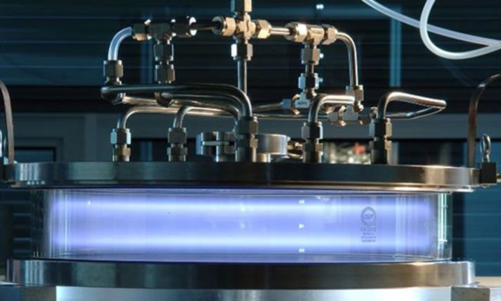
PECVD Process
The gases required for the reaction (precursor gases) are introduced into the reaction chamber through a precise gas flow control system. These gases typically include those used to form the main components of the film, such as silane (SiH₄) and oxygen (O₂) for depositing silicon oxide films, or silane and ammonia (NH₃) for depositing silicon nitride films. Auxiliary gases, such as argon (Ar), may also be introduced to adjust plasma properties or improve film quality.
Thin Film Deposition
Active species (radicals, ions, etc.) in the plasma diffuse toward the substrate surface and adsorb there. On the substrate surface, these active species undergo a chemical reaction, gradually forming a thin film. As the reaction continues, the film grows and gradually increases in thickness. By controlling parameters such as the reaction gas flow rate, plasma power, reaction chamber pressure, and substrate temperature, the film’s growth rate, composition, structure, and quality can be precisely controlled.
Exhaust Gas Treatment
The reaction produces gaseous byproducts such as hydrogen (H₂) and hydrogen chloride (HCl). These exhaust gases must be treated in a specialized exhaust gas treatment system to meet environmental emission standards. Common exhaust gas treatment methods include combustion, adsorption, and neutralization to ensure that the exhaust gases are environmentally friendly.
PECVD Types
RF-PECVD
RF-PECVD uses a radio frequency electric field to generate plasma and is categorized into RF inductive coupling and RF capacitive coupling. RF-PECVD uses an inductive coil to generate an alternating magnetic field, inducing a current in the reactant gas and generating plasma. RF-PECVD applies a radio frequency voltage between two parallel electrodes, ionizing the gas between the electrodes to form a plasma. RF-PECVD is widely used in fields such as semiconductors and optical thin films.
MW - PECVD
Using microwave-frequency electromagnetic fields to generate plasma. Microwave frequencies, typically in the GHz range, are more efficient at exciting gas molecules, producing a high-density, highly active plasma. MW-PECVD offers unique advantages in the production of high-quality diamond films, carbon nanotubes, and other materials because the plasma it generates provides a more uniform reaction environment, conducive to the growth of these specialized materials.
VHF - PECVD
VHF-PECVD uses a very high frequency (VHF, 30-300 MHz) electric field to generate plasma. Compared to traditional RF-PECVD, VHF-PECVD excites plasma electrons at lower temperatures and higher densities, significantly increasing the deposition rate of thin films. This allows for the production of desired thin films in a shorter time, improving production efficiency and finding widespread application in fields such as solar cells and flat-panel displays.
Advantages of PECVD
Low-Temperature Deposition
One of the greatest advantages of PECVD is its ability to deposit thin films at relatively low temperatures. This makes it suitable for use on temperature-sensitive substrates such as plastics, glass, and certain polymers.
Precise Thickness Control
By precisely controlling process parameters such as reaction time, gas flow rate, and plasma power, PECVD enables precise control of film thickness.
High-Quality Thin Films
The high activity of the plasma allows for more complete decomposition and reaction of the reactant gases, resulting in thin films with superior properties. These films typically exhibit higher purity, a denser structure, improved uniformity, and fewer defects.
Wide Material Applicability
PECVD can deposit thin films of a wide variety of materials, including various metals, inorganic films, and organic films. These range from common semiconductor materials (such as silicon and germanium) to various compound materials (such as nitrides, oxides, and carbides) and even organic polymers.
PECVD Applications
Plasma-enhanced chemical vapor deposition (PECVD), an advanced thin-film deposition technology, boasts a wide range of applications in fields such as semiconductor manufacturing, solar cells, display panels, optics, sensors, and MEMS, thanks to its unique principles and numerous advantages.
Semiconductors
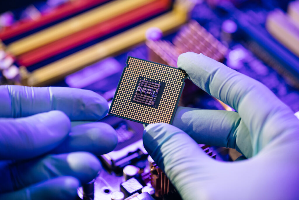
PECVD technology is ubiquitous in the semiconductor industry. It is used to deposit various insulating layers, passivation layers, and diffusion barriers. For example, in integrated circuit manufacturing, silicon oxide and silicon nitride films deposited by PECVD serve as insulating dielectrics, separating different conductive layers and preventing leakage. Silicon nitride films also serve as passivation layers, protecting the chip surface from environmental corrosion and improving chip reliability. Furthermore, in the manufacture of advanced semiconductor devices (such as FinFETs and 3D NAND flash memory), PECVD technology is used to deposit high-quality gate insulation layers and filler films in high-aspect-ratio structures, playing a key role in improving device performance and miniaturization.
Solar Cells
In the solar cell industry, PECVD technology is an important method for depositing critical thin films. For crystalline silicon solar cells, depositing a silicon nitride anti-reflection film on the surface of the silicon wafer using PECVD reduces light reflection, improves the cell’s light absorption efficiency, and thus enhances the cell’s photoelectric conversion efficiency. In thin-film solar cells (such as amorphous silicon, CIGS, and CdTe), PECVD is used to deposit functional thin films such as absorber and buffer layers, significantly impacting the cell’s performance and stability. For example, the intrinsic amorphous silicon thin film in amorphous silicon solar cells is typically produced using PECVD, and its quality directly impacts key parameters such as the cell’s open-circuit voltage and short-circuit current.

Display Panels
PECVD technology is used to deposit a variety of thin films in the manufacturing of liquid crystal displays (LCDs) and organic light-emitting diode displays (OLEDs). In LCDs, silicon nitride and silicon oxide films deposited via PECVD serve as insulating and passivation layers, protecting the liquid crystal molecules and driver circuitry. In OLEDs, PECVD-produced films encapsulate the organic light-emitting materials, preventing oxygen and moisture intrusion and improving the lifespan and stability of the OLED. Furthermore, in some emerging display technologies, such as quantum dot displays, PECVD can also be used to produce quantum dot films or other related functional films.

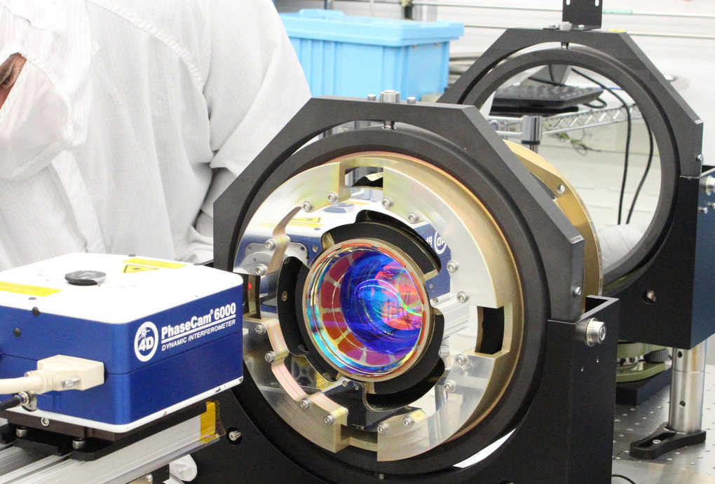
Optics
In the optical field, PECVD can be used to deposit various optical thin films, such as antireflection coatings, reflective coatings, and optical filters. These films utilize the optical properties of different materials. PECVD precisely controls the thickness and composition of the films, enabling precise control of light reflection, refraction, and absorption properties. For example, depositing an antireflection coating (AR) produced by PECVD on an optical lens can reduce light reflection loss, improving the lens’s transmittance and image quality. In laser devices, high-reflectivity films produced by PECVD serve as reflectors in the resonant cavity, playing a key role in laser generation and output.
Sensors
In sensor manufacturing, PECVD technology is used to produce sensitive thin films. For example, in gas sensors, PECVD is used to deposit thin films with adsorption and reactivity properties specific to specific gases. When target gas molecules adsorb on the film surface, the film’s electrical properties (such as resistance and capacitance) change, enabling gas detection. In other sensor types, such as pressure sensors and temperature sensors, PECVD-produced films can also play an important role as sensitive elements or structural support layers.
Microelectromechanical Systems (MEMS)
In the fabrication of MEMS devices, PECVD is used to deposit various structural and functional layers. For example, in inertial sensors like MEMS accelerometers and gyroscopes, thin films like silicon nitride and silicon oxide deposited via PECVD serve as structural layers to build micromechanical structures. These films also serve as insulating layers, isolating different conductive components. Furthermore, in some MEMS microphones and pressure sensors, thin films produced by PECVD can serve as sensitive materials, enabling the detection and conversion of physical quantities like sound and pressure.
Conclusion
Plasma-enhanced chemical vapor deposition (PECVD), with its unique principles and significant advantages, has demonstrated tremendous application value and development potential in numerous fields. From its initial application in semiconductor manufacturing to its current widespread penetration into cutting-edge fields such as solar cells, display panels, optics, and biomedicine, PECVD technology continues to drive advancements in materials science and related industries. With the continuous advancement of science and technology, research on PECVD technology continues to deepen, promising future breakthroughs in improving thin film performance, expanding application areas, and reducing production costs.