The Ultimate Guide to Reactive Sputtering
Reactive sputtering breaks through the limitations of traditional sputtering. Reactive gas is introduced into an inert gas environment, and a compound film with specific chemical composition and structure is generated on the substrate surface through chemical reactions between target atoms and reactive gas.
- Compounds: TiN, TiC, ZrO₂, etc.
- Metals: gold, silver, chromium, titanium, aluminum, etc.
- Alloys: nickel-chromium, cobalt-chromium, titanium-aluminum, etc.
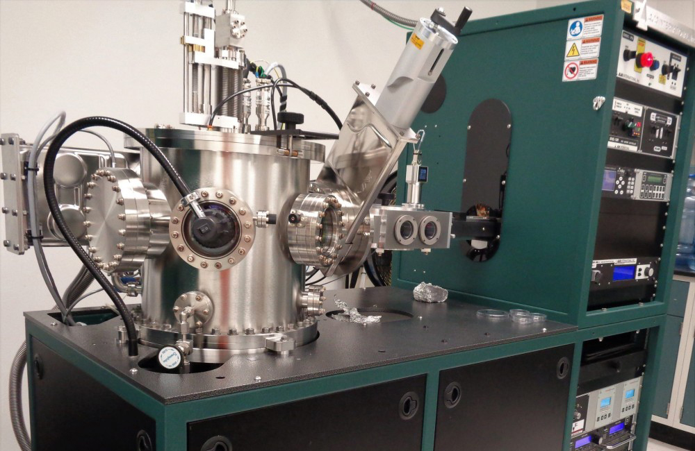
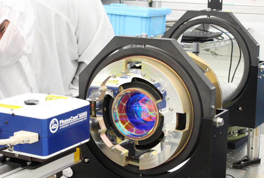
Wstitanium Workshop
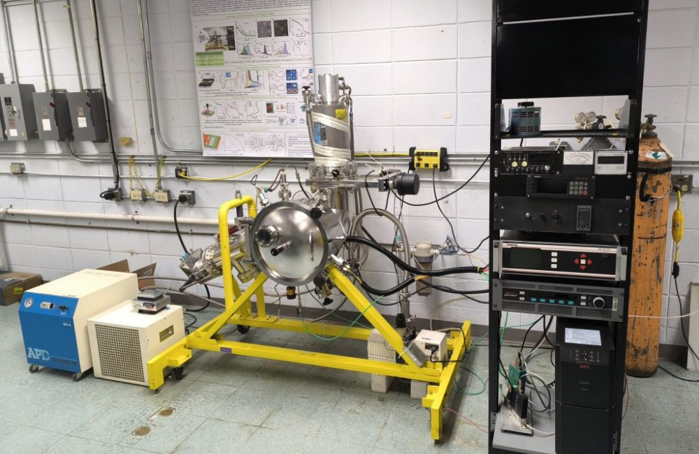
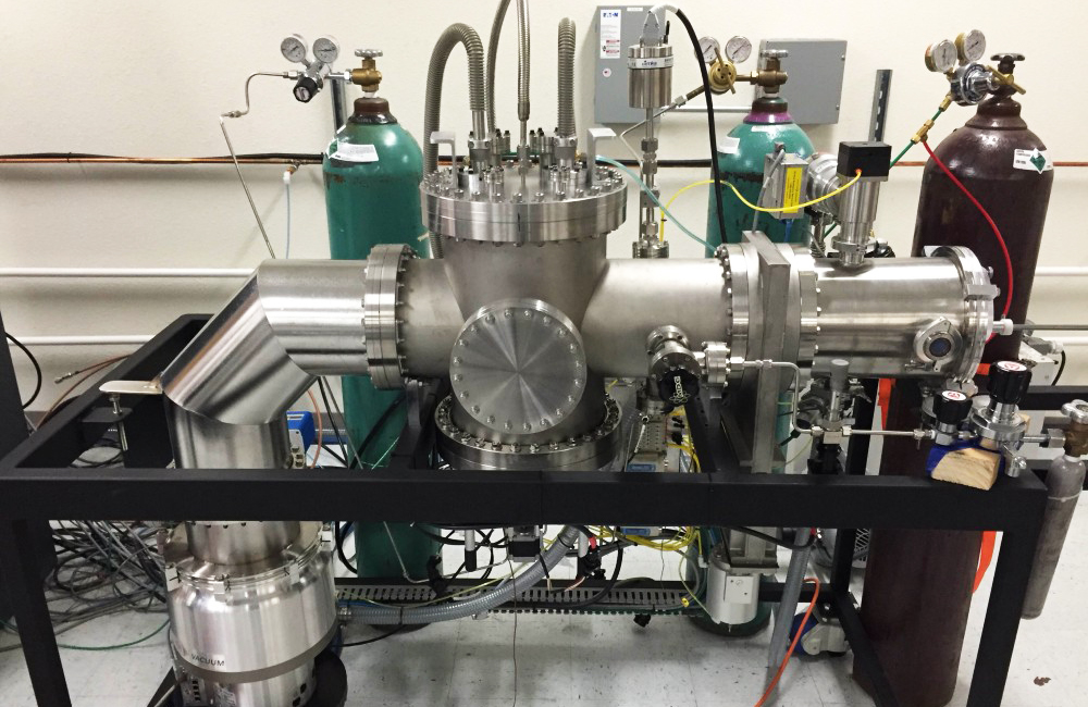
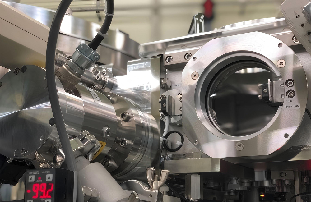
Our Powerful Facilities
Everything You Should Know About Reaction Sputtering
Reactive sputtering technology is everywhere, providing solid technical support for the development of many industries. A deep understanding of reactive sputtering technology will not only help you innovate in material research and development, but also provide a strong theoretical basis for you to optimize technology and improve film quality. This blog will comprehensively and in-depth explore all aspects of reactive sputtering, including its historical origins, working principles, modes, materials, technical advantages and disadvantages, and application areas, aiming to present you with a complete and clear picture of all information about reactive sputtering.
What is reactive sputtering?
Reactive sputtering is a type of physical vapor deposition (PVD) technology. In sputtering, in addition to using inert gases (such as argon Ar), reactive gases (such as oxygen O₂, nitrogen N₂, methane CH₄, etc.) are also introduced. In a high-energy plasma environment, the reactive gas reacts chemically with the atoms sputtered from the target to generate compounds, which are deposited on the surface of the substrate to form a thin film.
Traditional sputtering mainly sputters and deposits target atoms directly on the substrate to form a thin film with the same composition as the target. Reactive sputtering changes the chemical composition of the deposited film through chemical reactions, making it a compound film, which greatly expands the types and properties of thin film materials. For example, using a metal titanium target, reactive sputtering in a mixed atmosphere of argon and nitrogen can obtain a titanium nitride (TiN) film. Reactive sputtering in a mixed atmosphere of argon and oxygen can obtain a titanium dioxide (TiO₂) film.

Principle of Reactive Sputtering
In reactive sputtering, plasma needs to be generated in a vacuum chamber first. Usually, an inert gas (such as argon Ar) is used as the working gas. Then, an electric field (such as a DC electric field, a radio frequency electric field, or a pulsed electric field) is applied to ionize the argon atoms. Under the action of the electric field, the electrons are accelerated and collide with the argon atoms, knocking out the electrons in the argon atoms to form argon ions (Ar⁺) and free electrons, which form plasma. The particles in the plasma are in a high energy state and have high activity.
Target Sputtering
The generated argon ions bombard the target surface at high speed under the acceleration of the electric field. Because the ions have high kinetic energy, when they hit the target atoms, the momentum transfer allows the target atoms to obtain enough energy to escape from the target surface. This process is called sputtering. The sputtered target atoms exist in the vacuum chamber in a gaseous form and move in all directions. For example, when a metal copper target is used, argon ions bombard the copper target surface and sputter out copper atoms (Cu).
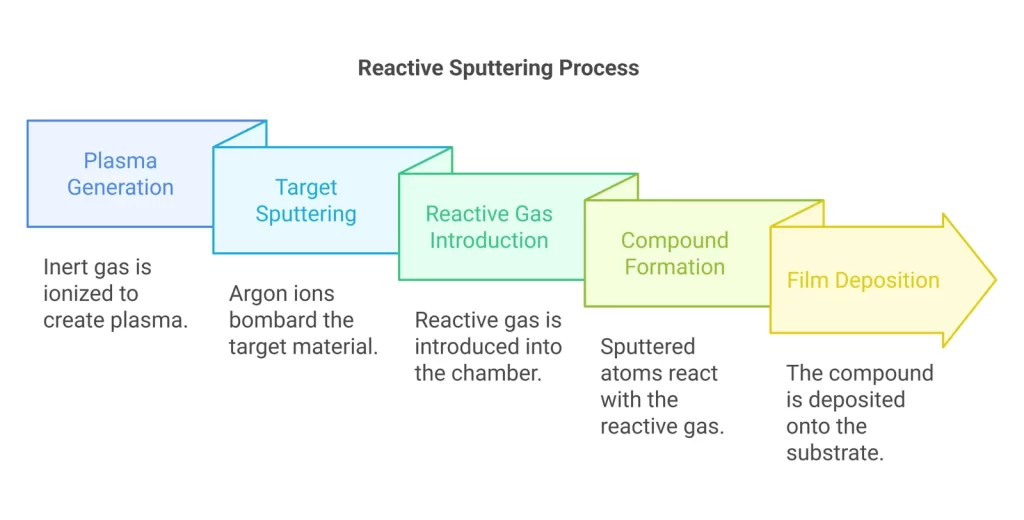
Reaction and Deposition
Reaction gases (such as oxygen O₂, nitrogen N₂, etc.) are introduced into the vacuum chamber. The sputtered target atoms and reaction gas molecules meet in the vacuum chamber and react chemically. Taking the preparation of oxide thin films as an example, if the target material is titanium (Ti) and the reaction gas is oxygen (O₂), the sputtered titanium atoms react with oxygen molecules to form titanium dioxide (TiO₂). The compounds generated by these reactions are eventually deposited on the substrate surface. The compound film gradually grows. During deposition, the growth rate, chemical composition and structure of the film are affected by many factors, such as reaction gas flow, sputtering power, substrate temperature, vacuum degree, etc.
Types of Reactive Sputtering
Different types of reactive sputtering technology have their own unique principles, working characteristics and application areas. DC reactive sputtering has the advantages of high deposition rate and simple equipment, but is susceptible to target poisoning. RF reactive sputtering solves the problem of sputtering of insulating targets, with high film quality but low rate and high cost. Magnetron reactive sputtering combines the advantages of high deposition rate and high-quality film. Pulse reactive sputtering can prepare high-quality films and flexibly control deposition. Medium-frequency reactive sputtering effectively solves the problem of target poisoning and has a high cost-effectiveness.
DC Reactive Sputtering
DC reactive sputtering is a relatively basic type of reactive sputtering technology. In a DC reactive sputtering system, the target acts as a cathode, and inert gas (such as argon Ar) and reactive gas (such as oxygen O₂, nitrogen N₂, etc.) are introduced into the system under a vacuum environment. When a DC voltage is applied between the target and the anode, the inert gas atoms are ionized, and the generated argon ions (Ar⁺) bombard the target surface at high speed under the acceleration of the electric field. After the target atoms gain enough energy, they are sputtered out from the target surface and enter the gas phase. The sputtered target atoms react chemically with the reactive gas to form compounds, which are finally deposited on the substrate to form a film.
RF Reactive Sputtering
RF reactive sputtering uses an RF power supply (usually at a frequency of 13.56MHz) to generate plasma. The electrons and ions in the plasma are alternately accelerated to move toward the target. In the positive half-cycle, electrons are attracted to the vicinity of the target material, neutralizing the positive charge while making the target material negatively charged; in the negative half-cycle, the working gas particles are attracted by the negative charge of the target material and move toward the target material, sputtering occurs, and coating is performed. Effective sputtering of insulator targets such as oxides and nitrides solves the problem that DC reactive sputtering cannot process insulating targets.
Magnetron Reactive Sputtering
Magnetron reactive sputtering is the preparation of compound thin films by introducing reactive gases on the basis of magnetron sputtering. The sputtered target atoms react chemically with the introduced reactive gases to deposit a compound thin film on the substrate. Due to the confinement of the magnetic field on electrons, the plasma density is greatly increased, the gas ionization is more sufficient, and the sputtering rate of the target atoms is significantly increased. The high plasma density and uniform sputtering environment make the deposited film have better uniformity, adhesion and density, and the structure of the film is more stable.
Pulse Reactive Sputtering
Pulse reactive sputtering uses a pulse power supply for sputtering coating, and controls the deposition rate and thickness of the film by adjusting parameters such as pulse width, frequency and duty cycle. In the high-power stage of the pulse, a short-term high-density plasma is generated, causing a large number of target atoms to sputter out; in the low-power stage, the reaction gas chemically reacts with the sputtered atoms and deposits on the substrate. Effectively reducing defects and stress in the film. The characteristics of the pulse power supply effectively control the charge accumulation on the target surface, reducing the occurrence of target poisoning and arcing.
Medium Frequency Reactive Sputtering
Medium frequency reactive sputtering uses a medium frequency power supply (usually between 1 and 200kHz) and solves the target poisoning and arcing problems in DC reactive sputtering by using two targets alternately as cathodes and anodes. In one cycle, when one target is sputtered as a cathode, the other target is used as an anode to collect electrons and neutralize the positive charge accumulated on the target surface, so that the sputtering process can proceed stably. This effectively avoids the target poisoning phenomenon caused by the accumulation of compounds on the target surface in DC reactive sputtering.
Examples of Materials Reactively Sputtered
| Compound Type | Initial Reactants | Compound Examples |
| Oxide | Metal target (e.g., Al, Ti, Zn, Sn, In, etc.) + Oxygen (O₂) | Aluminum oxide (Al₂O₃), Titanium dioxide (TiO₂), Zinc oxide (ZnO), Tin oxide (SnO₂), Indium oxide (In₂O₃) |
| Oxide | Alloy target (e.g., ITO alloy, Zn-Al alloy, etc.) + Oxygen (O₂) | Indium tin oxide (ITO, In₂O₃:Sn), Zinc aluminum oxide (ZnO:Al) |
| Nitride | Metal target (e.g., Ti, Cr, Zr, Ta, etc.) + Nitrogen (N₂) | Titanium nitride (TiN), Chromium nitride (CrN), Zirconium nitride (ZrN), Tantalum nitride (TaN) |
| Nitride | Semiconductor target (e.g., Si, Ge, etc.) + Nitrogen (N₂) | Silicon nitride (Si₃N₄), Germanium nitride (Ge₃N₄) |
| Carbide | Metal target (e.g., Ti, Cr, W, etc.) + Hydrocarbon gas (e.g., Methane CH₄, Acetylene C₂H₂, etc.) | Titanium carbide (TiC), Chromium carbide (Cr₃C₂), Tungsten carbide (WC) |
| Carbide | Carbon target (e.g., Graphite) + Metal target (e.g., Ti, Zr, etc.) + Argon (Ar) (Assisted sputtering) | Titanium carbide (TiC), Zirconium carbide (ZrC) |
| Sulfide | Metal target (e.g., Cd, Zn, Pb, etc.) + Hydrogen sulfide (H₂S) gas | Cadmium sulfide (CdS), Zinc sulfide (ZnS), Lead sulfide (PbS) |
| Sulfide | Metal sulfide target (e.g., MoS₂, etc.) + Argon (Ar) (Assisted sputtering, possibly with a small amount of reactive gas) | Molybdenum disulfide (MoS₂) |
| Fluoride | Metal target (e.g., Ca, Mg, Al, etc.) + Fluoride gas (e.g., Sulfur hexafluoride SF₆, etc.) | Calcium fluoride (CaF₂), Magnesium fluoride (MgF₂), Aluminum fluoride (AlF₃) |
| Fluoride | Metal fluoride target (e.g., LiF, etc.) + Argon (Ar) (Assisted sputtering) | Lithium fluoride (LiF) |
| Metal Compound | Metal target A (e.g., Cu) + Metal target B (e.g., Al) + Argon (Ar) (May contain a small amount of reactive gas to adjust properties) | Copper-aluminum alloy compound film (Different ratio compounds formed according to sputtering conditions) |
| Metal Compound | Metal target (e.g., Fe) + Rare earth element target (e.g., Nd) + Argon (Ar) (May contain reactive gas) | Neodymium-iron-boron (NdFeB)-related compound films (Used for special magnetic film preparation) |
Advantages of Reactive Sputtering
Stoichiometric ratio
Compound films with precise stoichiometric ratios are prepared by precisely adjusting the flow ratio of reactive gases (such as oxygen, nitrogen, etc.) and inert gases (such as argon).
Diversified films
Prepare a variety of compound films, and change the microstructure and composition of the films by adjusting parameters, thereby achieving diversified film performance.
Wide range of targets
Reactive sputtering uses various types of targets such as metals, alloys, semiconductors, and ceramics. Whether it is a single element target (such as pure titanium target, pure silicon target) or a complex alloy target.
Substrate material
Reactive sputtering deposits thin films on a variety of different substrate materials, including temperature-sensitive plastics, organic materials, etc., as well as traditional substrate materials such as metals, ceramics, and glass.
Good film uniformity
Reasonable design of the magnetic field distribution, gas flow distribution, and relative position of the target and substrate of the sputtering equipment can well control the thickness and composition uniformity of the film on a large area substrate.
High film purity
The target materials and reactive gases used in reactive sputtering are usually of high purity, which is conducive to the preparation of high-purity compound films. Ensure the performance and reliability of the chip.
High deposition rate
Especially the medium-frequency reactive sputtering mode has a high deposition rate, which meets the efficiency requirements of industrial large-scale. In the architectural glass coating industry, it is necessary to coat a large number of glass substrates with functional films in a short time. The high deposition rate of medium-frequency reactive sputtering makes large-scale production possible.
Realize continuous production
The reactive sputtering equipment is integrated with the automated production line to achieve continuous production. The automated control system accurately controls various parameters in sputtering, ensures the stability of film quality, improves production efficiency, and reduces production costs.
Disadvantages of Reactive Sputtering
Multiple parameters affect each other.
Reactive sputtering involves inert gas flow, sputtering power, substrate temperature, vacuum degree, etc. These parameters affect each other. To accurately control the performance of the film, these parameters need to be finely adjusted and optimized, which requires high technical level and experience of the operator.
Narrow process window
For the preparation of certain specific compound films, high-quality films can only be prepared within a specific parameter range. Beyond this range, it may cause problems such as imbalance of the stoichiometric ratio of the film, increase of structural defects, and performance degradation.
Target poisoning
Target poisoning principle: In reactive sputtering, especially DC reactive sputtering, the reactive gas reacts chemically with the atoms on the surface of the target material to form an insulating compound layer in the non-erosion area of the target surface. This is the target poisoning phenomenon.
High equipment cost
Reactive sputtering equipment usually needs to be equipped with complex components such as vacuum system, sputtering power supply (such as DC, RF, medium frequency power supply, etc.), gas flow control system, monitoring system, etc. The equipment is expensive.
Maintenance and operating costs
The maintenance of the equipment is relatively complicated, and it is necessary to regularly check and maintain the sealing of the vacuum system, clean the sputtering target and vacuum chamber, calibrate the gas flow control system, etc.
Pollution
Some reaction gases are dangerous, such as hydrogen sulfide (H₂S), which is a highly toxic gas. Sulfur hexafluoride (SF₆) is a toxic substance that may be decomposed at high temperatures. Safety operating procedures must be strictly followed.
Application of Reactive Sputtering
As an important thin film preparation technology, reactive sputtering has unique principles and diverse working modes. It can prepare a wide variety of compound films and show broad application prospects and great practical value in many fields.
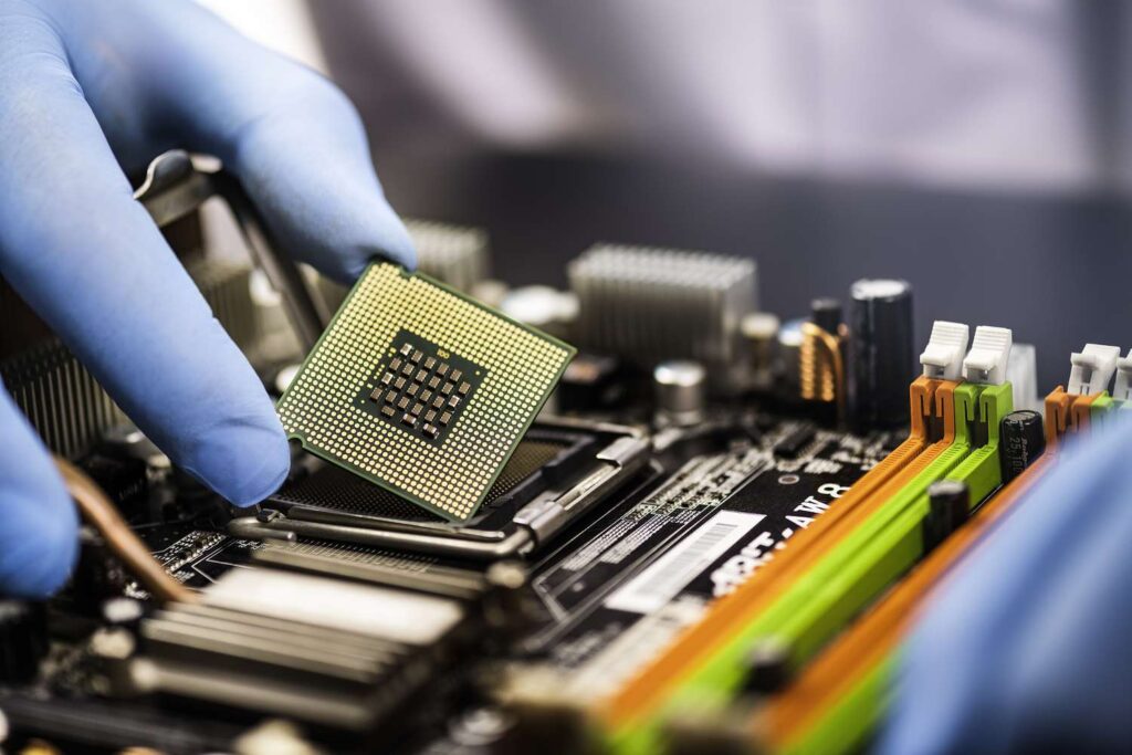
Electronics
In integrated circuit manufacturing, reactive sputtering is widely used to prepare various thin film materials, such as metal interconnection layers, insulating layers and barrier layers. Reactive sputtering deposits high-quality metal films, such as copper (Cu), aluminum (Al), etc. on silicon wafers, which are used to make interconnection lines in integrated circuits and realize electrical connections between different devices inside the chip. At the same time, insulating films such as silicon nitride (Si₃N₄) and silicon dioxide (SiO₂) prepared by reactive sputtering are used as insulating layers in chips. In addition, barrier layer films such as titanium nitride (TiN) are used to prevent the diffusion of metal atoms and ensure the performance and reliability of integrated circuits.
Optics
Reactive sputtering is an important method for preparing various optical films, such as anti-reflection films, reflective films, filter films, etc. For example, reactive sputtering deposits one or more layers of thin films such as silicon dioxide and magnesium fluoride (MgF₂) on the surface of glass lenses, which significantly reduces the reflectivity of the lenses within a specific wavelength range. In the manufacture of reflectors, the reflectivity of reflectors can be improved by depositing metal films (such as silver Ag, aluminum Al, etc.) or metal oxide films (such as titanium dioxide TiO₂, etc.) through reactive sputtering.
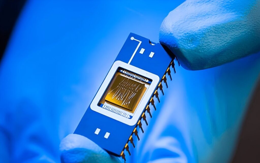
Optoelectronic
In the manufacture of light-emitting diodes (LEDs), compound semiconductor films such as gallium nitride (GaN) are deposited on substrates such as sapphire by reactive sputtering as the light-emitting layer of LEDs. In the manufacture of laser diodes (LDs), reactive sputtering can be used to prepare semiconductor gain medium films, optical cavity mirror films, etc. In addition, in the manufacture of photodetectors, films such as lead sulfide (PbS) and cadmium selenide (CdSe) prepared by reactive sputtering can be used as light absorption layers to detect and convert light signals.
Material Surface Modification
Reactive sputtering can also be used to modify the surface of materials and improve the surface properties of materials. Depositing a ceramic film, such as aluminum oxide (Al₂O₃) and zirconium oxide (ZrO₂), on the surface of metal materials by reactive sputtering can improve the corrosion resistance and high temperature resistance of metal materials. Depositing metal films or metal oxide films on the surface of plastic materials can give plastic materials new properties such as conductivity and electromagnetic shielding. In addition, depositing bioactive films, such as hydroxyapatite (HA), on the surface of biomedical materials by reactive sputtering can improve the biocompatibility of materials and promote cell adhesion and growth.

Conclusion
In principle, reactive sputtering cleverly combines sputtering and chemical reactions, accurately controls plasma, target sputtering, and each link of chemical reactions, and realizes precise control of film composition and structure. In terms of application, reactive sputtering provides key thin film preparation technology for integrated circuits, flat panel displays, and sensor manufacturing in the field of electronics and semiconductors, supporting the rapid development of the modern electronics industry; in the field of optics, it is used to prepare various optical films and optoelectronic devices, promoting the progress of optical technology; in the field of mechanical and material surface engineering, by preparing hard coatings and modifying the surface of materials, the performance of mechanical parts and the service life of materials are improved. However, reactive sputtering technology is not perfect. Its technical complexity makes parameter control difficult, and the target poisoning problem is still one of the important factors restricting its further development. The equipment cost and maintenance requirements are high, and the safety and environmental protection of reactive gases cannot be ignored.
References
- Musil, Jindrich, Jaroslav Vlcek, and Pavel Baroch. “Magnetron discharges for thin films plasma processing.” Materials Surface Processing by Directed Energy Techniques 1 (2006): 67-110.
- Bishop, Charles. Vacuum deposition onto webs, films and foils. William Andrew, 2011.
- https://en.wikipedia.org/wiki/Sputter_deposition
Licari, James J. Hybrid microcircuit technology handbook: materials, processes, design, testing and production. Chapter 3. Thin Film Processes, Elsevier, 1998.