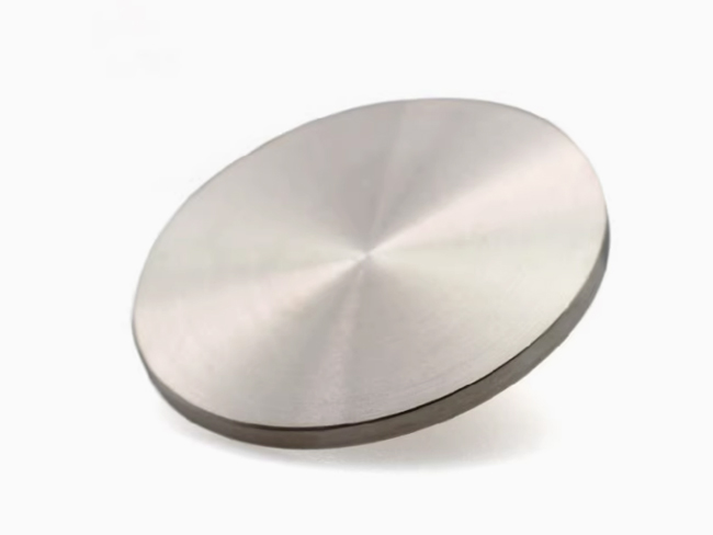
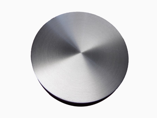
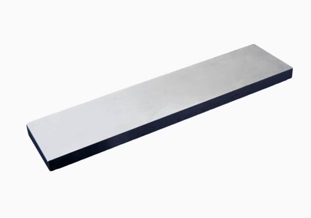
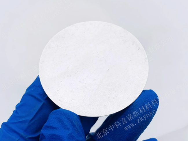
Sputtering Coating
With its unique advantages and wide applicability, sputtering coating has been deeply applied in many fields. From precise metal wiring in microelectronic devices to high-performance coatings on optical components; from high-temperature protective layers in the aerospace field to decorative coatings on daily necessities, sputtering coating technology is everywhere and has a profound impact on the progress of science and technology.
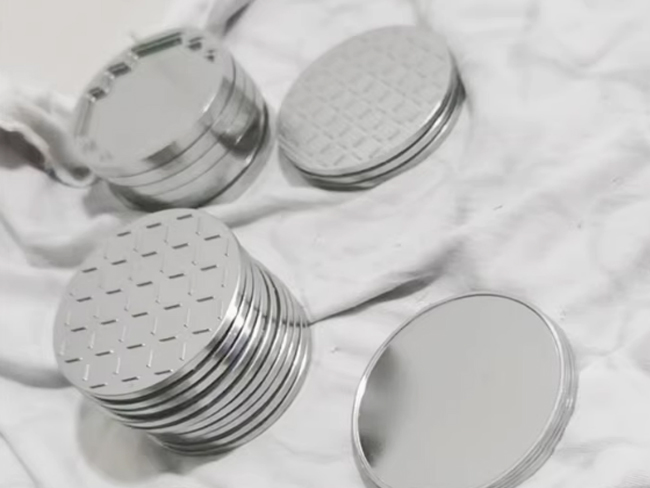
Wstitanium Workshop
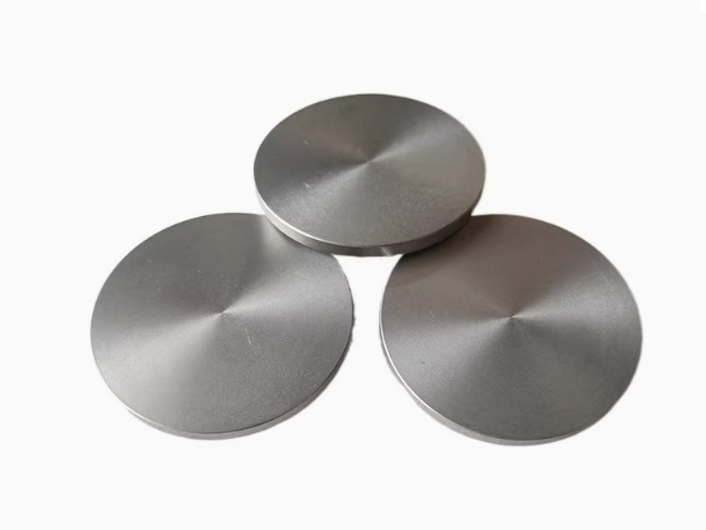
Our Powerful Facilities
Everything You Should Know About Sputtering Coating
With the rapid development of science and technology, the requirements for material performance are increasing day by day, and sputtering coating technology is also constantly innovating and improving. New sputtering methods are constantly emerging. The options for coating materials are more abundant and diverse. The accuracy and stability of technical control have been greatly improved. This enables sputtering coating to not only meet the needs of traditional fields, but also provide key thin film preparation solutions for emerging technology fields such as quantum computing, flexible electronics, biomedical engineering, etc.
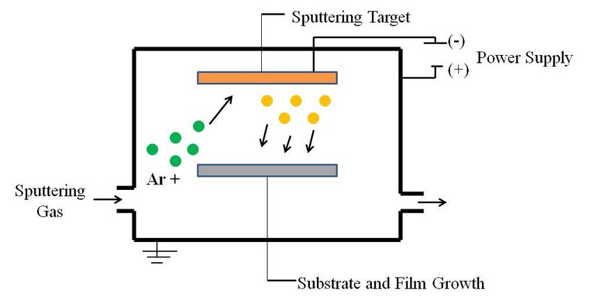
Sputtering coating is a physical vapor deposition (PVD) technology. Its basic principle is to bombard the target surface with high-energy ions (usually argon ions Ar⁺) in a vacuum environment, so that the target atoms gain enough energy to overcome the surface binding force and escape. These escaped atoms are deposited on the substrate surface and gradually form a thin film. This process involves complex physical phenomena, including ion generation, ion acceleration, momentum transfer, and atomic deposition.
Sputtering Working Mechanism

Ion generation and acceleration: Inert gas (such as argon) is introduced into the vacuum chamber, and the gas is ionized by applying an electric field (usually using glow discharge) to generate plasma, which contains a large number of argon ions and free electrons. Argon ions are accelerated under the action of the electric field and obtain higher kinetic energy. For example, in a DC sputtering device, a DC voltage is applied between the target (cathode) and the anode to form an electric field, which accelerates the argon ions to fly toward the target.
Momentum transfer and atomic sputtering: When argon ions with high kinetic energy bombard the target surface, they collide elastically or inelastically with the target atoms, transferring their own kinetic energy to the target atoms. When the energy obtained by the target atoms exceeds their binding energy in the lattice, they will sputter out from the target surface. In elastic collisions, ions collide directly with target atoms and transfer kinetic energy instantly; in inelastic collisions, multiple energy exchanges are used to gradually allow the target atoms to obtain enough energy and sputter.
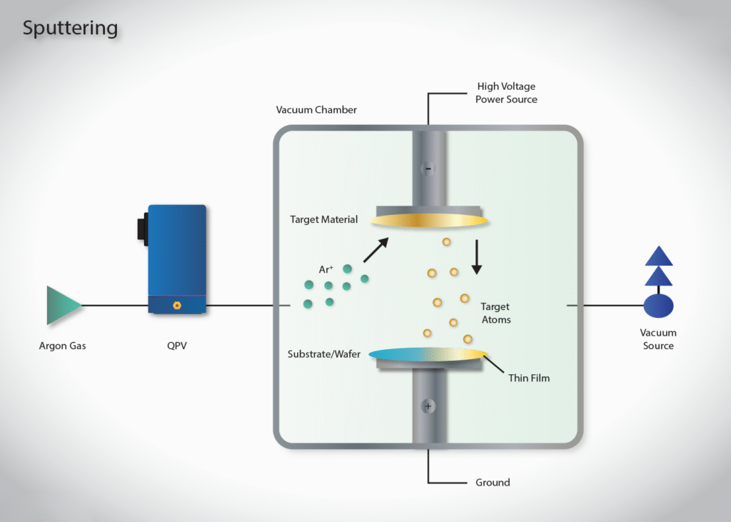
Atomic deposition and film growth: The atoms sputtered from the target are transported in a vacuum chamber in a gaseous form and deposited on the substrate surface. These atoms adsorb and diffuse on the substrate surface, gradually forming atomic clusters. As the number of deposited atoms increases, the clusters continue to grow and connect to each other, eventually forming a continuous film. The growth process of the film is affected by many factors, such as the deposition rate of atoms, substrate temperature, and the diffusion ability of atoms on the substrate surface.
Sputtering vs. Evaporation
Evaporation is the process of evaporating the coating material by heating it, and then the vapor condenses on the substrate surface to form a film. Compared with sputtering, evaporation usually has a higher deposition rate, but poorer coverage of complex-shaped substrates. Because the movement direction of the evaporated atoms is mainly straight, it is difficult to evenly cover all parts of the substrate. In addition, evaporation has limited selectivity for materials, and some high-melting-point materials are difficult to coat. Sputtering can be carried out at a lower temperature and is suitable for temperature-sensitive substrate materials. The sputtered particles have higher energy and can interact strongly with the substrate surface, so that the film has good adhesion to the substrate.
Sputtering vs. CVD
CVD uses gaseous chemicals to react chemically under high temperature and catalysts to generate solid substances and deposit them on the substrate surface to form thin films. CVD can produce high-quality films and can precisely control the chemical composition and crystal structure of the film. However, CVD usually requires a high temperature environment, which may damage the substrate material and may introduce impurities during the reaction process. Sputtering coating does not require high temperature chemical reactions, avoiding the problems caused by high temperature and chemical reactions. It can achieve coating of almost all solid materials, and the equipment is relatively simple and the cost is low.
History of Sputtering Coating
The development of sputtering coating technology is a history of scientific and technological progress full of innovation and breakthroughs. Its origin can be traced back to the 19th century. In 1852, German physicist William Grove observed the sputtering phenomenon for the first time. When he was conducting a gas discharge experiment, he found that when ions bombarded the surface of a metal electrode, metal atoms would detach from the electrode surface and deposit on the surrounding objects. This accidental discovery laid the foundation for the birth of sputtering coating technology.
Early Development Stage
In the decades after Grove discovered the sputtering phenomenon, scientists conducted in-depth research on the basic principles and characteristics of sputtering. In 1902, German scientist Eugen Goldstein further studied the sputtering process and revealed the relationship between the emission mechanism of sputtering atoms and factors such as ion energy and target material. These early studies provided a theoretical basis for the practical application of sputtering coating technology, but due to the limitations of technical conditions at the time, sputtering coating could not be achieved in large-scale industrial production.
Technological Breakthroughs
In the mid-20th century, with the development of vacuum technology, power technology and materials science, sputtering coating technology has made major breakthroughs. The emergence of RF sputtering technology has solved the problem of sputtering coating of insulating materials, which has greatly expanded the application scope of sputtering coating technology. RF sputtering uses the alternating electric field generated by the RF power supply to ionize the gas, thereby realizing the sputtering of insulating target materials. This technology has been widely used in fields such as integrated circuits.
Modern Development Trend
In the 21st century, with the continuous advancement of science and technology, sputtering coating technology has continued to make progress in improving coating quality, reducing costs, and expanding application areas. New sputtering technologies such as pulsed DC sputtering and high-power pulsed magnetron sputtering (HiPIMS) continue to emerge. Pulsed DC sputtering reduces the formation of an insulating layer on the surface of the target material by superimposing high-frequency pulses on the DC voltage, alleviates the target material poisoning phenomenon, and improves the stability and quality of the coating. HiPIMS can generate plasma with a high ionization rate and prepare thin films with excellent performance, showing great application potential in high-end optical films, superhard coatings and other fields.
Sputtering Coating Type
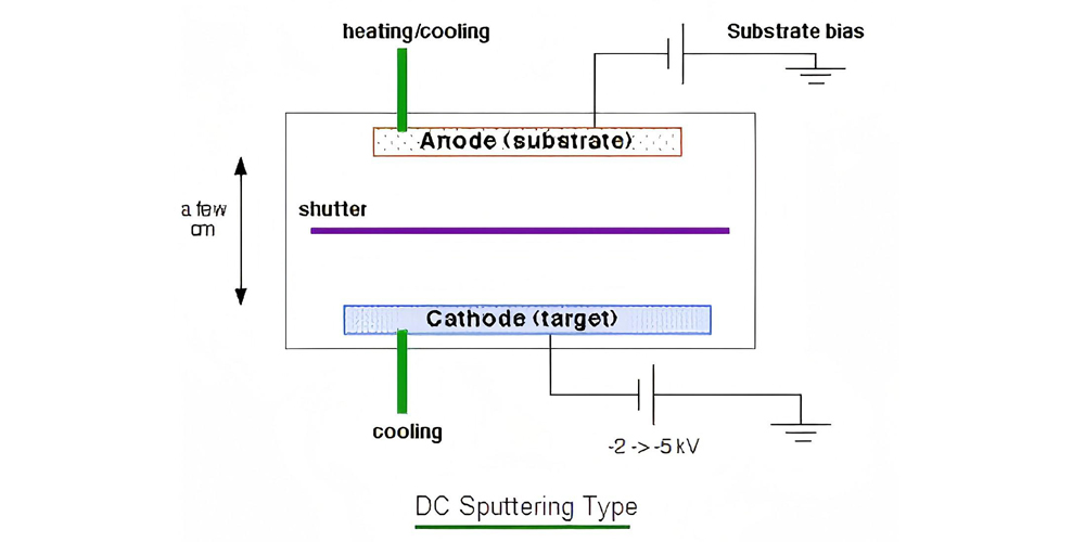
DC sputtering is a technology that uses ions generated by DC glow discharge to bombard the target material for sputtering coating. DC sputtering is relatively low in cost and is suitable for large-area uniform coating. However, it also has some limitations. Since DC sputtering requires the target material to have good conductivity, it can only be used for coating conductive materials, and cannot be used for insulating materials.
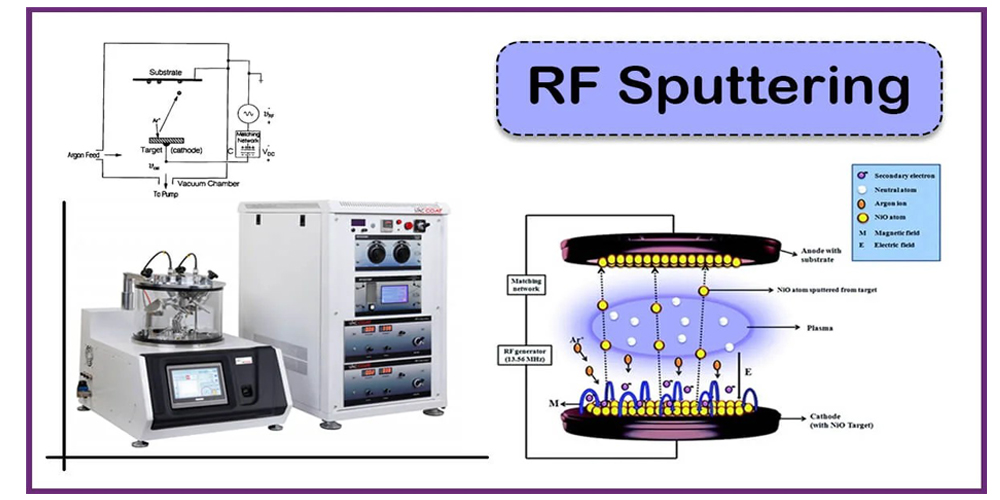
RF Sputtering
RF sputtering is a technology that uses positive ions in RF discharge plasma to bombard the target material, sputter out target atoms and deposit them on the surface of a grounded substrate. RF sputtering can be used to deposit thin films of almost any solid material, including conductors, semiconductors and insulators. The thin films it obtains are dense, high in purity and firmly attached to the substrate.
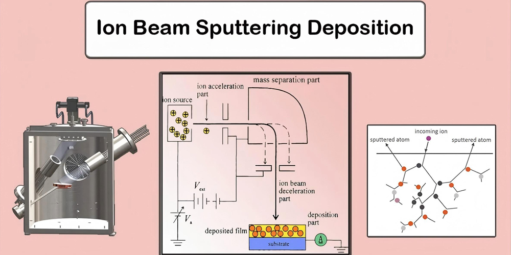
Ion Beam Sputtering
Ion beam sputtering is a technology that uses an independent ion source to generate a high-energy ion beam, directly bombarding the target surface, so that the target atoms are sputtered out and deposited on the substrate to form a thin film. The ion source usually uses a Kaufman ion source or a radio frequency ion source to accelerate the ions to a higher energy.
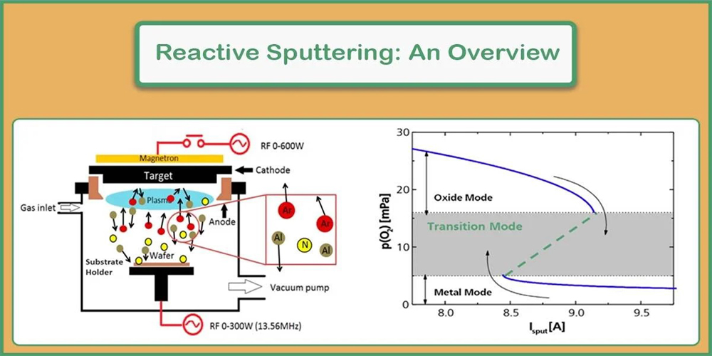
Reactive Sputtering
Reactive sputtering is a technology in which reactive gases (such as oxygen, nitrogen, methane, etc.) are introduced into the vacuum chamber during the sputtering process to react chemically with the sputtered target atoms to form a compound film on the substrate surface. Reactive sputtering is widely used in the preparation of various compound films, such as oxides, nitrides, carbides, etc.
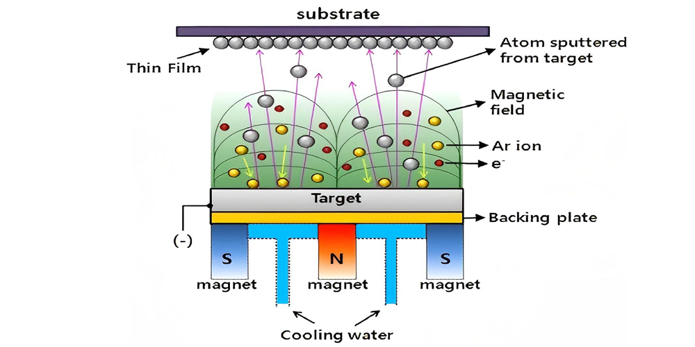
Magnetron Sputtering
Magnetron sputtering is a technology that establishes a racetrack magnetic field on the cathode target surface, uses it to control the movement of secondary electrons, prolongs their residence time near the target surface, increases the probability of collision with the gas, and thus increases the plasma density. It can be carried out at a lower working pressure.
Pulse DC Sputtering
Pulse DC sputtering is to superimpose high-frequency pulses on the basis of DC voltage. Its power supply periodically outputs pulse signals while providing stable DC output to reduce target poisoning. Pulse DC sputtering is suitable for reactive sputtering processes and can effectively improve the stability of the coating process and the quality of the film. It reduces impurities and defects in the film.
Sputtering Yield
Sputtering yield, also known as sputtering coefficient, refers to the average number of target atoms sputtered from the target surface by each incident ion during the sputtering process, usually represented by Y. It is an important parameter for measuring the efficiency of sputtering coating, which directly affects the deposition rate and preparation cost of the film. The energy of sputtered atoms varies greatly, and usually the kinetic energy of these atoms exceeds tens of electron volts (usually 600 eV). About one percent of the ions hit the target surface with ballistic impact and return to the substrate, resulting in re-sputtering. The size of the sputtering yield depends on many factors, including the energy and type of the incident ions, the properties of the target (such as atomic mass, crystal structure, binding energy, etc.), and the working conditions during sputtering (such as gas pressure, temperature, etc.).
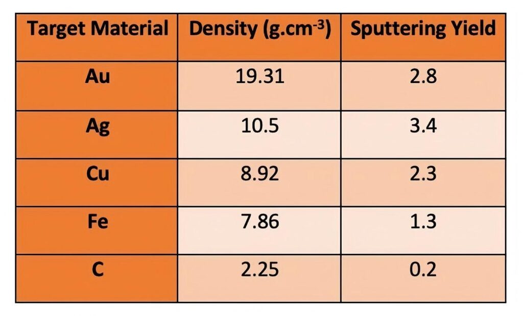
Table 1. Sputtering Yield of Different Materials for 600 eV Ion Energy
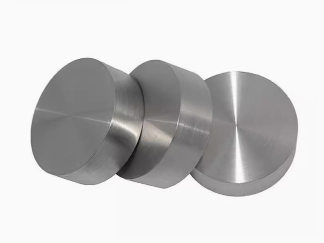
The choice of sputtering materials, as the core element of magnetron sputtering, directly determines the properties and application range of the film. Different sputtering materials, due to their unique physical, chemical and electrical properties, can produce films with different functions and characteristics. For example, metal materials are often used to prepare conductive films, metal decorative films and wear-resistant coatings in electronic devices due to their good conductivity, high sputtering rate and excellent mechanical properties; alloy materials can obtain films with special properties by cleverly adjusting the proportion of different metal elements, such as high strength, high corrosion resistance or special electrical and magnetic properties, and are widely used in high-end fields such as aerospace and automobile manufacturing; ceramic materials, with their high hardness, high temperature resistance and strong chemical stability, perform well in the preparation of optical films, insulating films and protective coatings, providing strong support for the performance improvement of optical instruments and electronic equipment.
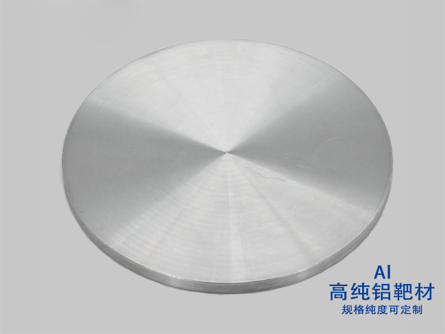
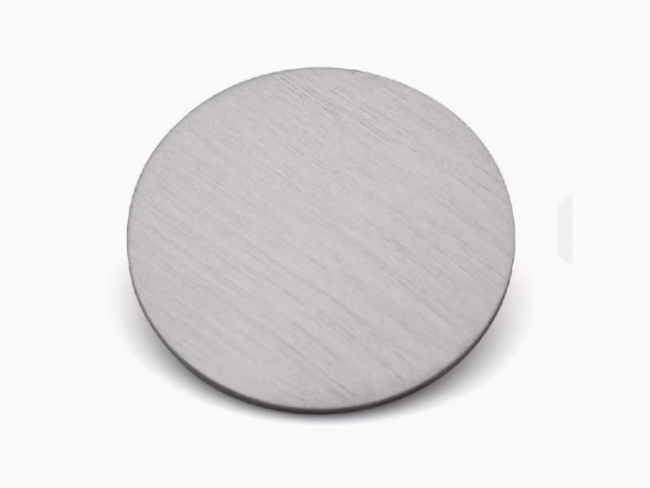
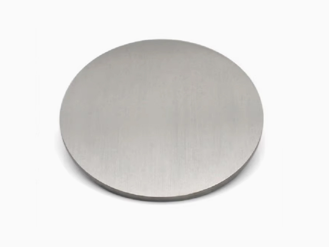
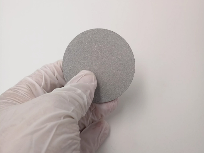
Aluminum (Al) Sputtering Target
Aluminum is a widely used sputtering metal material. It has low density and good electrical conductivity. Its density is about 2.7g/cm³, and its room temperature conductivity can reach 3.77×10⁷S/m. In the field of electronic devices, aluminum is often used to prepare metal wiring in integrated circuits. Aluminum films are widely used in optical instruments such as telescopes and microscopes.
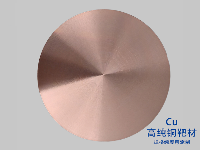
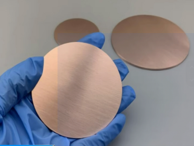
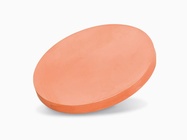
Copper (Cu) Sputtering Target
Copper has excellent electrical conductivity, with an electrical conductivity of up to 5.96×10⁷S/m. In ultra-large-scale integrated circuits, copper has gradually replaced aluminum as the mainstream metal wiring material due to its low resistance characteristics. Copper also has good thermal conductivity and good electrical conductivity, and effectively shields electromagnetic interference.
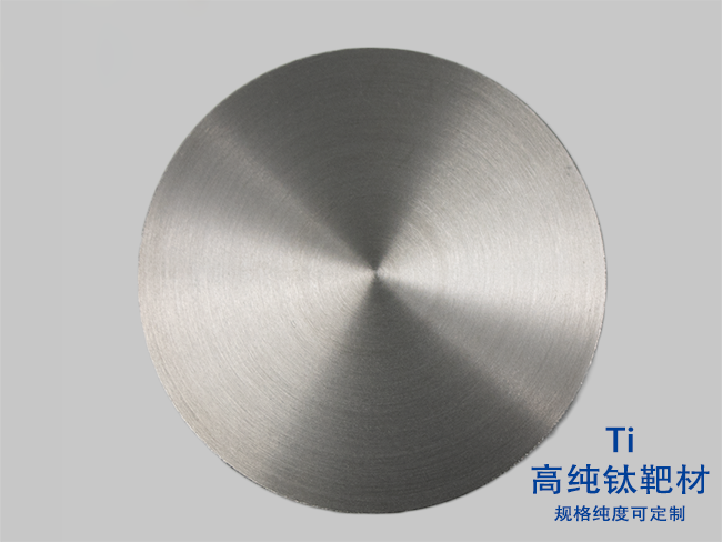
Titanium (Ti) Sputtering Target
Titanium has a high melting point (1668℃) and good mechanical properties. Its density is 4.506g/cm³, that is, the ratio of strength to density is large. Sputtering titanium film can improve the wear resistance, corrosion resistance and high temperature resistance of parts. Titanium also has excellent biocompatibility. Titanium film can also be used for anti-corrosion coatings.
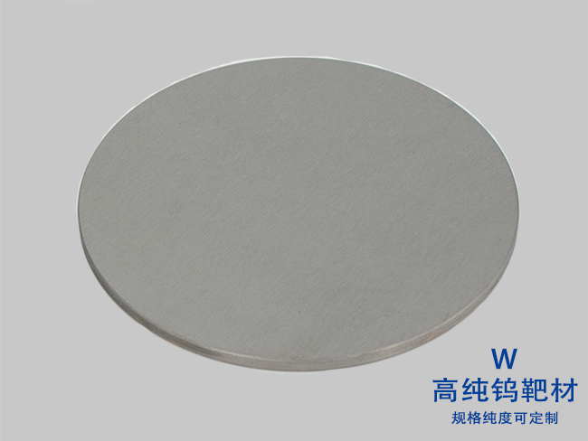
Tungsten (W) Sputtering Target
Tungsten has an extremely high melting point of 3422℃, one of the highest melting points of all metals. This makes it have excellent stability in high temperature environments. Sputtered tungsten film can be used as a high temperature protective coating. Sputtered tungsten film can be used to coat tools to improve the cutting performance and service life of the tools.
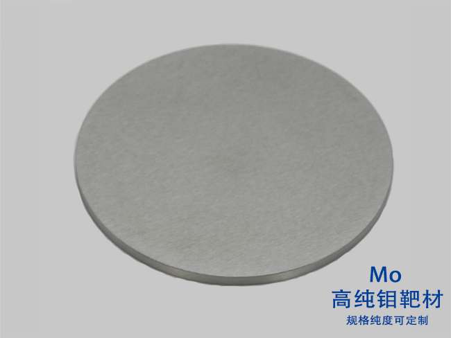
Molybdenum (Mo) Sputtering Target
Molybdenum has good high-temperature performance and can still maintain high strength and stability at high temperatures. Molybdenum is one of the important materials for manufacturing thin-film transistors (TFTs). Sputtered molybdenum film is used as the electrode and wiring material of TFTs. In the field of solar cells, molybdenum film is used as the back electrode material.
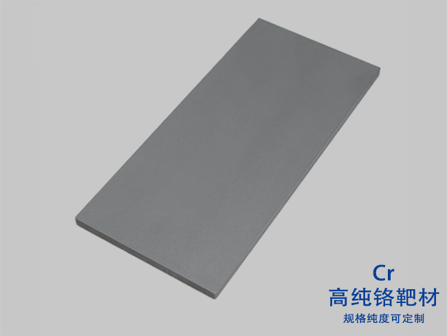
Chromium (Cr) Sputtering Target
Chromium has a high hardness, Mohs hardness of about 9, and good wear resistance. Sputtering chromium film significantly improves the surface hardness and wear resistance of parts. Chromium also has good corrosion resistance and can remain stable in a variety of chemical environments. Chromium film has a bright metallic appearance and is often used for surface decoration.
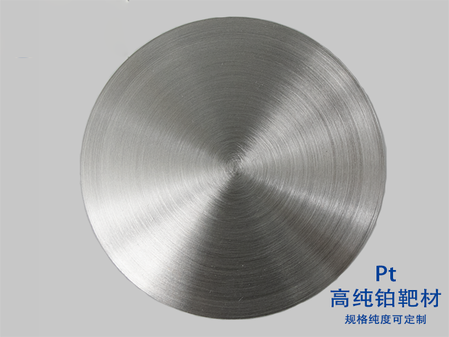
Platinum (Pt) Sputtering Target
Platinum has extremely high chemical stability and catalytic activity. In the field of fuel cells, platinum catalysts are one of the core materials of proton exchange membrane fuel cells (PEMFC). In the field of electronic devices, platinum is often used to make high-end electronic components, such as electrodes and resistors in integrated circuits.
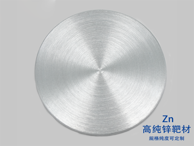
Zinc (Zn) Sputtering Target
Zinc has good corrosion resistance. Sputtering zinc film on the surface of steel to form a galvanized layer is a common method for steel corrosion protection. It is widely used in construction, automobiles, bridges and other fields. Zinc is the negative electrode material of common batteries such as zinc-manganese batteries and zinc-air batteries. Zinc film is also used in the field of decoration.
Rhodium (Rh) Sputtering Target
Rhodium has good catalytic and antioxidant properties. Many important chemical reactions (such as hydrogenation and dehydrogenation reactions in organic synthesis) require the participation of rhodium catalysts. By sputtering rhodium film on the surface of the catalyst carrier, the dispersion and catalytic activity of rhodium can be improved, and the chemical reaction can be promoted.
Nickel (Ni) Sputtering Target
Nickel has good corrosion resistance and can remain stable in many chemical media and is not easily corroded. Nickel film can be used to enhance the mechanical strength and reliability of components, and its good conductivity also helps the transmission of electronic signals. Nickel-based alloy films are widely used in the manufacture of storage media such as hard disks and magnetic tapes.
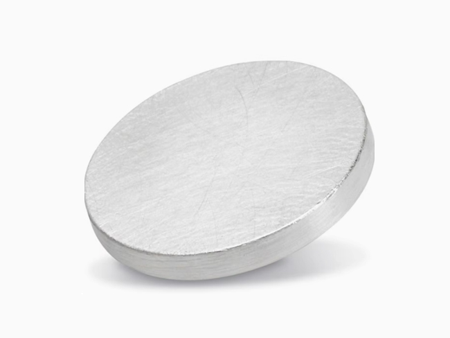
Silver (Ag) Sputtering Target
Silver has the highest conductivity among all metals, with an electrical conductivity of 6.30×10⁷S/m. Silver film has very high reflectivity in the visible and near-infrared bands and is widely used to make high-quality reflectors. Silver also has good antibacterial properties, which makes it uniquely used in biomedicine and food packaging. However, the chemical stability of silver is relatively poor.
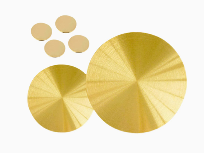
Gold (Au) Sputtering Target
Gold has extremely high chemical stability, hardly reacts chemically with other substances, and can maintain good performance in various harsh environments. Its good conductivity and oxidation resistance make it an ideal coating material for key parts in electronic devices. In the jewelry industry, sputtering gold film can achieve a gold-like decorative effect on the surface of other metals or materials.
Tantalum (Ta) Sputtering Target
Tantalum has excellent chemical stability and shows good corrosion resistance in most chemical media, especially in highly corrosive acid and alkali environments. Sputtered tantalum film can provide reliable corrosion protection. Tantalum also has good biocompatibility. Sputtered tantalum film is also used to manufacture electrode materials for tantalum capacitors.
Niobium (Nb) Sputtering Target
Sputtering niobium film can be used to prepare superconducting thin films for the manufacture of superconducting quantum interference devices (SQUIDs), superconducting filters, etc. These devices play a key role in biomedical detection, communications, quantum computing, etc. The corrosion resistance of niobium makes it a corrosion-resistant coating material.
Palladium (Pd) Sputtering Target
Palladium has good catalytic properties and is used as a catalyst. Sputtering palladium film on the surface of the carrier material increases the surface area of palladium and improves the catalytic activity. Palladium is often used to make electrodes and connecting materials for electronic components. Sputtering palladium film achieves decorative effects on other metal surfaces.
Ruthenium (Ru) Sputtering Target
Sputtering ruthenium film on the surface of the catalyst carrier achieves more efficient and environmentally friendly chemical production. Ruthenium is also commonly used to manufacture electronic components such as resistors and capacitors. Sputtering ruthenium film or related ruthenium compound film can optimize the photoelectric conversion performance of the battery.
Cobalt (Co) Sputtering Target
Cobalt has good magnetic properties and is one of the important elements for making permanent magnetic materials. Sputtered cobalt film can prepare high-performance permanent magnetic films for micro motors, micro speakers, etc. Cobalt is also commonly used to manufacture metal interconnect materials in integrated circuits. Cobalt-based alloys have certain biocompatibility.
Iridium (Ir) Sputtering Target
Iridium has an extremely high melting point (2446℃) and chemical stability. Sputtered iridium film can provide excellent high temperature protection and corrosion resistance. Iridium is often used to manufacture high-end electronic components, such as electrodes and interconnect materials in integrated circuits. Iridium is also an important material for making reference electrodes.
Tin (Sn) Sputtering Target
Tin has a low melting point (231.9℃) and good ductility. Sputtering tin film can accurately control the thickness and composition of the solder, improve the reliability and precision of welding, and meet the needs of miniaturization and high-density packaging of electronic devices. Sputtering tin oxide film can prepare transparent conductive films.
Lead (Pb) Sputtering Target
Sputtering lead film can be used to prepare radiation protection materials for medical and nuclear industries, such as X-ray shields and protective layers of nuclear reactors, which effectively block the harm of radiation to the human body and the environment. Sputtering lead film can optimize the structure and performance of electrodes.
Iron (Fe) Sputtering Target
Iron-based alloy films (such as iron-silicon alloys and iron-nickel alloys) are widely used in the manufacture of transformer cores, inductor components, etc. Sputtering iron-based alloy films can accurately control the magnetic parameters of the film (such as magnetic permeability, coercivity, etc.) and improve the performance of magnetic components.
Zirconium (Zr) Sputtering Target
Sputtered zirconium film can protect equipment from corrosion by strong acids, strong alkalis and other corrosive media, and improve the reliability and service life of the equipment. Zirconium has a small thermal neutron absorption cross-section and is an important cladding material for nuclear reactor fuel rods.
Hafnium (Hf) Sputtering Target
Sputtered hafnium film can be used as a high-temperature protective coating to protect components from damage in extremely high temperature environments. In the nuclear industry, hafnium has a strong absorption capacity for thermal neutrons and is an important material for nuclear reactor control rods.
Indium (In) Sputtering Target
Sputtered indium film can achieve reliable connection between electronic components, especially suitable for electronic packaging in low temperature environments. Indium tin oxide (ITO) is an important transparent conductive material. Sputtered ITO film (containing indium) can be used to prepare electrodes and touch screens for displays.
Gallium (Ga) Sputtering Target
Gallium-based semiconductor materials (such as gallium arsenide GaAs, gallium nitride GaN) are widely used in the manufacture of high-frequency, high-speed electronic devices and optoelectronic devices. Sputtering gallium film or related gallium compound film can prepare the key layer of semiconductor devices.

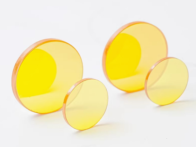
MgF₂ Sputtering Target
Magnesium fluoride has a low refractive index and good light transmittance. Sputtering MgF₂ film can reduce the reflected light on the surface of optical components and is used in optical instruments such as eyeglass lenses, camera lenses, and telescopes. MgF₂ film can be used for optical coatings of laser devices to improve the output efficiency of lasers.
Al-Cu Sputtering Target
Aluminum-copper combines the lightweight of aluminum and the high conductivity of copper. Sputtered Al-Cu film is used as a metal wiring material in integrated circuits. Its good conductivity and anti-electromigration properties ensure the stable transmission of electronic signals and are suitable for the manufacture of high-performance chips.
Ti - Al Sputtering Target
Titanium-aluminum has a high melting point, low density and good high temperature performance. Sputtering Ti – Al alloy film can be used as a high temperature protective coating to improve the oxidation resistance and wear resistance of parts at high temperatures. In the automotive industry, Ti – Al alloy film can be used to manufacture surface coatings for engine valves, pistons and other parts.
Cu - Ni Sputtering Target
Copper-nickel alloy has good conductivity and stable resistance performance. Sputtering Cu – Ni film can accurately control the resistance value and temperature coefficient of the component. Cu – Ni alloy has excellent seawater corrosion resistance, and sputtering Cu – Ni film can be used for surface protection of ship hulls, pipelines and other components.
Fe-Ni Sputtering Target
Fe-Ni alloy has high magnetic permeability and low coercivity, and is widely used in manufacturing transformer cores, magnetic shielding materials, magnetic sensors, etc. Sputtering Fe-Ni film can prepare ultra-thin magnetic films, which are suitable for microelectronic devices and high-frequency magnetic components.
Co-Cr Sputtering Target
Cobalt-chromium has good wear resistance, corrosion resistance and biocompatibility. Sputtering Co-Cr alloy film can improve the surface hardness and wear resistance of the device. In the field of aerospace, Co-Cr alloy film can be used to manufacture surface coatings for engine bearings, gears and other parts.
W - Mo Sputtering Target
Tungsten-molybdenum has a high melting point, good high temperature strength and conductivity, and is often used to manufacture cathode and anode materials for high temperature electron tubes, X-ray tubes and other equipment. Sputtering W – Mo alloy film can improve the high temperature resistance and electron emission efficiency of the electrode.
Al - Si Sputtering Target
Aluminum-silicon is often used to manufacture surface coatings for engine cylinders, pistons and other parts. Sputtering Al – Si film can improve the wear resistance and corrosion resistance of parts. In the field of electronic packaging, Al – Si alloy film can be used as a surface coating for packaging materials.
Ti-Ni Sputtering Target
Titanium-nickel gold is a shape memory alloy with unique shape memory effect and superelasticity. It is often used to manufacture orthopedic instruments, dental braces, etc. Sputtering Ti-Ni alloy film can prepare medical devices with shape memory function.
CIGS Sputtering Target
Copper indium gallium selenide is an important semiconductor material. Sputtering CIGS film is used to prepare the absorption layer of solar cells. Precisely control the sputtering technical parameters to optimize the electrical and optical properties of the film and improve the conversion efficiency of solar energy.

SiO₂ Sputtering Target
Silicon dioxide has good insulation, light transmittance and chemical stability, and is often used to manufacture anti-reflection films and high-reflection films for optical lenses. Sputtering SiO₂ film can reduce light reflection and improve the transmittance of lenses. It is widely used in optical instruments such as glasses and camera lenses.
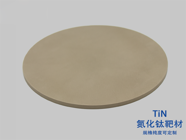
TiN Sputtering Target
Titanium nitride has high hardness, high wear resistance, good conductivity and golden appearance. TiN film coated tools have excellent cutting performance. TiN films can be used as electrode materials and diffusion barriers. Their good conductivity and stability can meet the needs of devices.
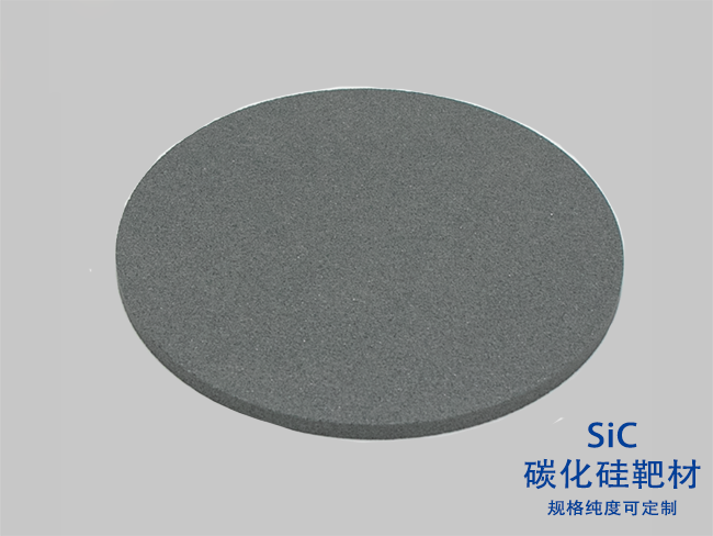
SiC Sputtering Target
Silicon carbide has high hardness, high melting point, good thermal conductivity and semiconductor properties. Sputtering SiC films can be used to prepare epitaxial layers and buffer layers of devices. SiC films can be used for surface coatings of components such as tools and bearings to improve their wear resistance and service life. SiC film can be used as thermal protection coating for spacecraft.

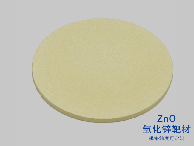
ZnO Sputtering Target
Zinc oxide has good semiconductor, piezoelectric and optical properties. ZnO film can be used to make varistors, thin film transistors, etc. ZnO film has good light transmittance in the ultraviolet band and can be used to make optoelectronic devices such as ultraviolet detectors and light-emitting diodes. ZnO film can be used to make gas sensors, humidity sensors, etc.
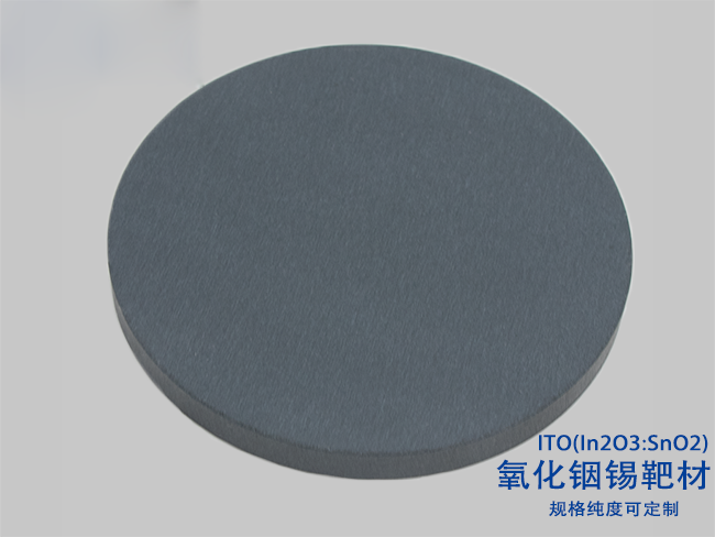
ITO Sputtering Target
Indium tin oxide is a transparent conductive material with high transmittance and high conductivity. In the display field, ITO film is a key material for touch screens, liquid crystal displays and other devices. In the field of electromagnetic shielding, ITO film can be used to make transparent electromagnetic shielding materials, which are suitable for display windows of precision electronic equipment.
AlN Sputtering Target
Aluminum nitride has high thermal conductivity, good insulation and high temperature resistance. AlN film can be used as a high thermal conductivity insulating layer. AlN has excellent piezoelectric properties and can be used to manufacture surface acoustic wave devices (SAW), bulk acoustic wave devices (BAW), etc., and is widely used in communications, radar and other fields.
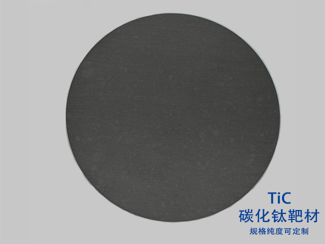
TiC Sputtering Target
Titanium carbide has extremely high hardness, wear resistance and melting point. The cutting performance of TiC film coated tools is better than that of traditional tools. TiC film can be used for mold surface coating to improve the wear resistance and anti-seizure of the mold. TiC film can be used as a protective coating for high-temperature parts to resist high temperature and friction wear.

TiO₂ Sputtering Target
Titanium dioxide has excellent optical properties, photocatalytic properties and chemical stability. TiO₂ films can be used as coatings for optical components such as high-reflection films and interference filters. Sputtering TiO₂ films can be used to prepare self-cleaning materials, such as self-cleaning glass and self-cleaning tiles.
ZrO₂ Sputtering Target
Zirconium oxide has a high melting point, high hardness and good phase change properties. Sputtering ZrO₂ film can further improve the surface properties of ceramic materials. ZrO₂ film has low thermal conductivity and high melting point. Zirconia has good biocompatibility and corrosion resistance and can be used to make artificial joints, dental restorations, etc.
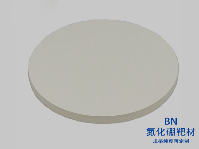
BN Sputtering Target
Boron nitride has structures such as hexagonal boron nitride (h-BN) and cubic boron nitride (c-BN). h-BN has good lubricity, high temperature resistance and insulation. h-BN film can be used as a high-temperature lubricant coating. c-BN has extremely high hardness and wear resistance, close to diamond. BN film can be used as an insulating layer and heat dissipation layer.

BaTiO₃ Sputtering Target
Barium titanate is an important ferroelectric material with high dielectric constant and good ferroelectric properties. It is often used to manufacture ceramic capacitors, ferroelectric memory, etc. Sputtering BaTiO₃ film can prepare high-performance dielectric films, improve the capacity of capacitors and the storage performance of ferroelectric memory.

SnO₂ Sputtering Target
Tin oxide has good conductivity, light transmittance and chemical stability. In the field of gas sensors, SnO₂ film is a commonly used gas-sensitive material with high sensitivity to a variety of reducing gases (such as methane, propane, hydrogen, etc.). SnO₂ film can be used as a transparent electrode for solar cells, a heat reflective film for glass, etc.

LiNbO₃ Sputtering Target
Lithium niobate has good piezoelectric, electro-optical and nonlinear optical properties. LiNbO₃ film can be used to manufacture optical waveguides, optical modulators and other devices, and is a key material in optical communication systems. LiNbO₃ film can be used to manufacture surface acoustic wave devices and nonlinear optical materials.

SiC Sputtering Target
Silicon carbide has high hardness, high melting point, good thermal conductivity and semiconductor properties. Sputtering SiC film can prepare the epitaxial layer and buffer layer of the device, which is suitable for manufacturing radio frequency devices, etc. SiC film can be used as a thermal protection coating for spacecraft.

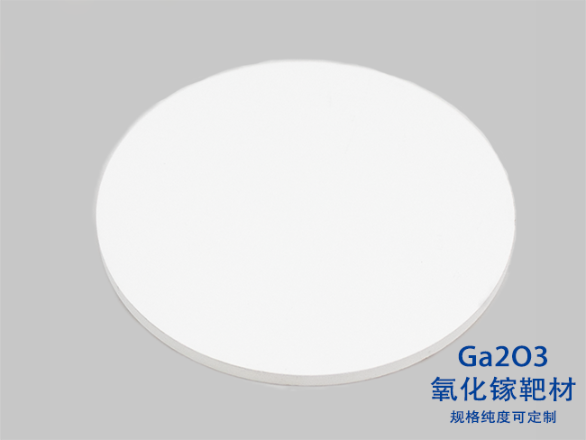
Ga₂O₃ Sputtering Target
Gallium oxide is a wide bandgap semiconductor material with excellent breakdown field strength and thermal conductivity. Ga₂O₃ film can be used to manufacture high-voltage power devices such as Schottky barrier diodes, metal-oxide-semiconductor field effect transistors, etc. Ga₂O₃ film can be used to manufacture ultraviolet detectors, etc.

In₂O₃ Sputtering Target
Indium oxide has good conductivity and light transmittance, and is often doped with tin to form ITO (indium tin oxide). In₂O₃ film can be used for the window layer of solar cells, transparent electrodes of displays, etc. In₂O₃ film is sensitive to certain gases (such as carbon monoxide, ethanol, etc.), and gas sensors can be prepared by sputtering.
MgO Sputtering Target
Magnesium oxide has good insulation, high temperature resistance and chemical stability. MgO film can be used as a protective layer for plasma display panels (PDP). MgO film can be used as a sintering aid for ceramic materials to improve the microstructure and mechanical properties of ceramics. Sputtering MgO film can improve the dispersion and stability of catalysts and enhance catalytic activity.

Al₂O₃ Sputtering Target
Alumina has high hardness, high melting point, good insulation and corrosion resistance. Sputtering Al₂O₃ film can improve the surface hardness and wear resistance of ceramic materials. Al₂O₃ film can be used as an insulating layer, protective layer, etc. Al₂O₃ film can be used as a surface coating for artificial joints, orthopedic implants, etc.

Si₃N₄ Sputtering Target
Silicon nitride has high strength, high hardness, good high temperature resistance and insulation. Sputtering Si₃N₄ films can protect the surface of semiconductor devices. Sputtering Si₃N₄ films can further optimize the surface properties of ceramics. Si₃N₄ films can be used as coating materials for optical films to adjust the refractive index and reflectivity of optical components.
ZnS Sputtering Target
Zinc sulfide has good light transmittance. ZnS film is an important infrared window and lens material, widely used in infrared detection, thermal imaging and other equipment. ZnS film can be used as a coating material for anti-reflection film and filter to optimize the performance of optical components. In addition, ZnS can be used to manufacture light-emitting diodes, phosphors, etc.
Ni-Cr Sputtering Target
Sputtering Ni-Cr alloy film can improve the heating efficiency and service life of electric heating elements. Ni-Cr alloy film can be used as a resistor material with a small resistance temperature coefficient and good stability. Ni-Cr alloy has certain biocompatibility and can be used to manufacture surface coatings for artificial joints, dental instruments, etc.
ZnSe Sputtering Target
Zinc selenide has excellent light transmittance in the infrared band. ZnSe film is often used to manufacture optical components such as infrared lenses and prisms, and is suitable for equipment such as carbon dioxide lasers and infrared remote sensing. ZnSe is a II-VI compound semiconductor that can be used to manufacture optoelectronic devices such as blue light-emitting diodes.
InP Sputtering Target
Indium phosphide is an important III-V compound semiconductor with high electron mobility and good optical properties. InP film can be used to manufacture optoelectronic devices such as lasers and photodetectors. InP can be used to manufacture microwave radio frequency devices, which are used in radar, communications and other fields.

LiTaO₃ Sputtering Target
Lithium tantalate has excellent piezoelectric, electro-optical and pyroelectric properties. LiTaO₃ film can be used to manufacture surface acoustic wave devices (SAW), which are used in communications, radar, electronic countermeasures, etc. LiTaO₃ film can be used as a material for electro-optical modulators, infrared detectors, temperature sensors, etc.
VN Sputtering Target
Vanadium nitride has high hardness, high wear resistance and good conductivity. VN film coated tools can improve the cutting performance and service life of tools. VN film has a golden to dark gray appearance and can be used for surface decoration. VN film can be used as a diffusion barrier and electrode material.
Sputtering Coating Advantages
Wide Material Adaptability
Sputtering coating can coat almost all solid materials, including metals, alloys, compounds, semiconductors, etc., without being restricted by the melting point, conductivity and other properties of the material. For example, for metals with high melting points such as tungsten and molybdenum, as well as insulating compounds such as silicon dioxide and aluminum oxide, it can meet the needs of various material films in different fields.
Thin Film Performance Excellent
The film prepared by sputtering coating has high density and good adhesion. Because the sputtered atoms have high energy, they can interact strongly with the substrate when deposited on the substrate surface, forming a strong bond, reducing the risk of peeling between the film and the substrate. At the same time, the film has good composition uniformity, and the thickness of the film can be precisely controlled, and the error can be controlled at the nanometer level.
Low Temperature Coating Capability
Compared with some coating technologies that require high temperature environments (such as chemical vapor deposition), sputtering coating can be carried out at lower temperatures, and the substrate temperature can usually be controlled in the range of room temperature to several hundred degrees Celsius. This feature makes sputtering coating suitable for temperature-sensitive substrate materials, such as plastics, polymers, semiconductor wafers, etc.
Strong controllability
The parameters of sputtering coating (such as sputtering power, gas pressure, target-substrate distance, substrate temperature, etc.) can be precisely controlled to effectively regulate the composition, structure, thickness, performance, etc. of the film. This good controllability enables sputtering coating to be mass-produced, and the product has high repeatability and stability. For example, a film with a specific refractive index and thickness can be prepared.
Sputtering Coating Application
In the field of electronic information, magnetron coating is a key preparation technology for metal interconnection layers and dielectric layers in chip manufacturing, supporting the development of semiconductor devices towards miniaturization and high integration. In the field of new energy, it provides a protective layer for the electrode surface of lithium-ion batteries, improves the cycle life and safety of batteries, and promotes the progress of electric vehicles and energy storage technology. In the field of aerospace, the thermal insulation coating on the surface of spacecraft and the reflective film of satellite antennas all rely on magnetron coating to achieve stable operation in extreme environments. In the field of biomedicine, by coating the surface of implantable medical devices with biocompatible films, the body’s rejection reaction can be effectively reduced, allowing artificial joints, heart stents and other equipment to serve patients more safely.
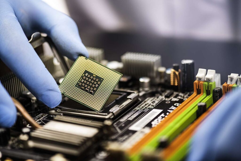
Electronics and Semiconductor Field
In integrated circuits, sputtering is used to prepare key structures such as metal wiring, gate electrodes, and contact layers. For example, metal films such as aluminum and copper are deposited on the surface of semiconductor wafers by sputtering, and serve as conductive wiring to transmit electronic signals; insulating films such as silicon dioxide and silicon nitride serve as interlayer insulating layers and passivation layers to achieve electrical isolation and protection of devices. The high precision and high uniformity of sputtering can meet the needs of continuous size reduction and increased integration of integrated circuits, and is one of the core processes in chip manufacturing. In flat panel display devices such as liquid crystal displays (LCDs) and organic light-emitting diode displays (OLEDs), sputtering is used to prepare transparent conductive films (such as ITO films), electrode materials, isolation layers, etc.
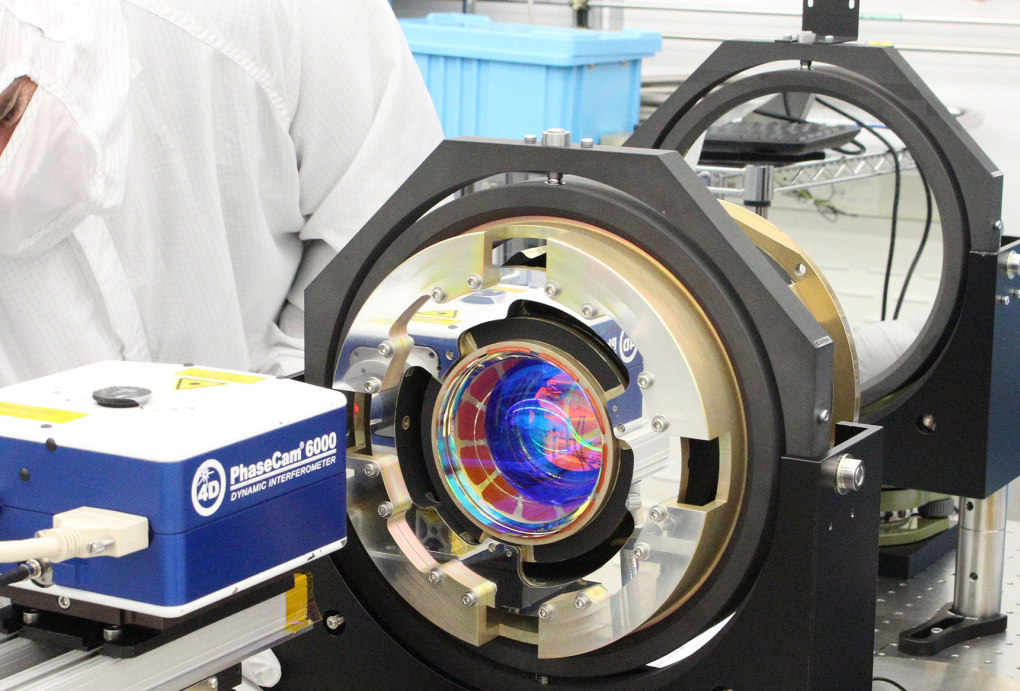
Optical Field
Sputtering is widely used in the preparation of various optical films, such as anti-reflection films, high-reflection films, filters, etc. Anti-reflection films (such as silicon dioxide and magnesium fluoride films) are used to reduce light reflection on the surface of optical components and improve light transmittance. They are used in eyeglasses, camera lenses, telescopes, etc. High-reflection films (such as aluminum, silver, and gold films) are used to reflect light of specific wavelengths and manufacture reflectors, laser resonators, etc. Filters are used to selectively transmit or reflect light of specific wavelengths through the combination of multiple layers of sputtered films. They are used in spectral analysis, communications and other fields. Sputtering coating is used to prepare films for infrared optical windows, lenses, prisms and other devices. Films such as zinc sulfide and zinc selenide have good infrared transmittance.
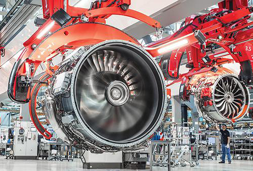
Aerospace and Energy Field
The engine parts and spacecraft structures in the aerospace field need to withstand extreme environments such as high temperature, high pressure, and corrosion. High-temperature protective coatings (such as tungsten, molybdenum, and zirconium oxide films), wear-resistant coatings (such as silicon carbide films), and anti-corrosion coatings (such as aluminum and chromium films) prepared by sputtering coating can effectively protect these parts and improve their reliability and service life. For example, the thermal barrier coating (zirconia-based) on the surface of turbine blades can reduce the temperature of the blades and prevent high-temperature damage.
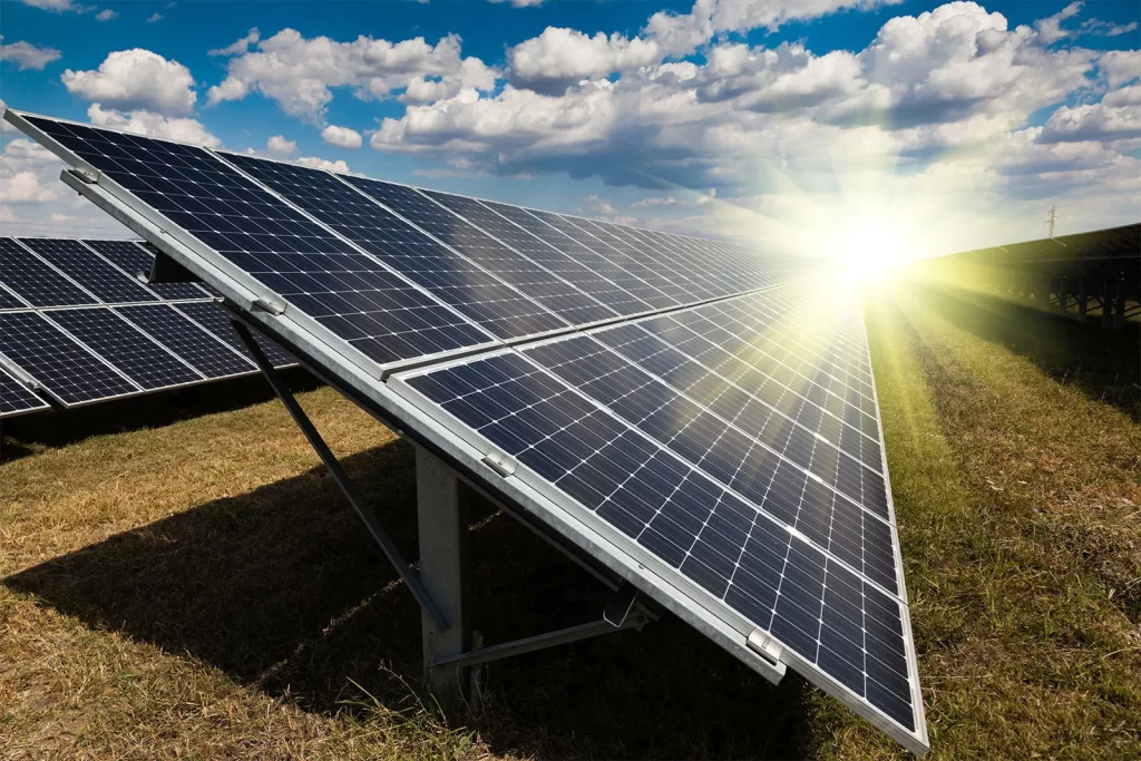
Solar Cells
In the manufacture of solar cells, sputtering coating is used to prepare electrode materials, absorption layers, window layers, etc. For example, copper indium gallium selenide (CIGS) thin films are deposited by sputtering as the absorption layer of solar cells, efficiently absorbing sunlight and converting it into electrical energy; metal films such as aluminum and silver are used as back electrodes and front electrodes to collect and transmit current; transparent conductive films such as zinc oxide and indium oxide are used as window layers to allow light to enter the absorption layer while exporting current. Sputtering coating can improve the photoelectric conversion efficiency and stability of solar cells and promote the development of the solar energy industry.
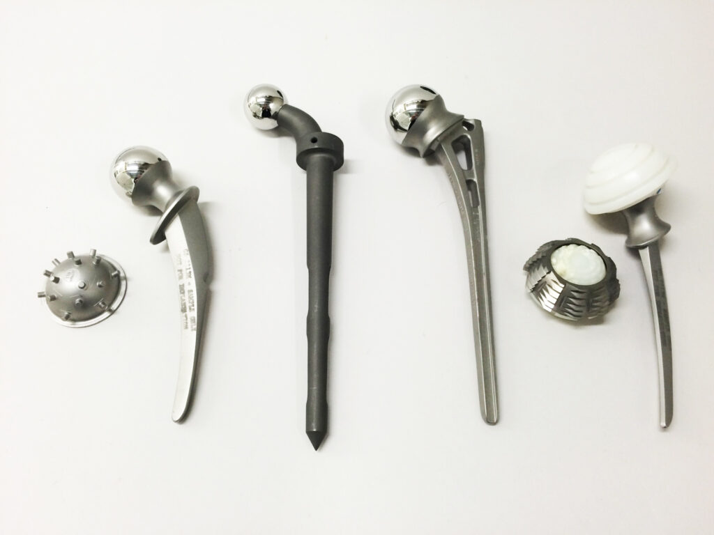
Medical
On the surface of medical devices such as artificial joints, dental implants, and heart stents, biocompatible films (such as titanium, titanium nitride, and zirconium oxide films) prepared by sputtering can improve the surface properties of the device, improve its compatibility with human tissues, reduce rejection reactions, and promote tissue healing. For example, artificial joints coated with titanium films have good biocompatibility and wear resistance, which can improve the service life of joints and the quality of life of patients.
Biosensors
Sputtering coating is used to prepare electrode materials and sensitive films for biosensors. Metal films such as gold and platinum are used as electrodes to provide a stable electrochemical interface; specific compound films (such as titanium dioxide and boron nitride) are used as sensitive films to specifically identify biological molecules (such as proteins, DNA, glucose, etc.), achieving high-sensitivity detection of biological samples, and are used in medical diagnosis, biological analysis and other fields.
Conclusion
As an important physical vapor deposition technology, sputtering coating plays an irreplaceable role in many fields such as electronics and semiconductors, optics, decoration and protection, aerospace, energy, biomedicine, etc., relying on its wide material adaptability, excellent thin film performance, low-temperature coating ability, good step coverage and controllable process. From the basic principle, sputtering coating bombards the target material with high-energy ions to cause atoms to escape and deposit into a film. The process involves multiple links such as ion generation, acceleration, momentum transfer and atomic deposition. After years of development, sputtering coating has derived various types such as DC sputtering, RF sputtering, reactive sputtering, magnetron sputtering, ion beam sputtering, pulsed DC sputtering, etc.