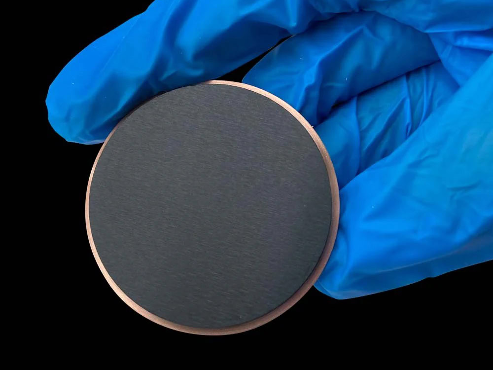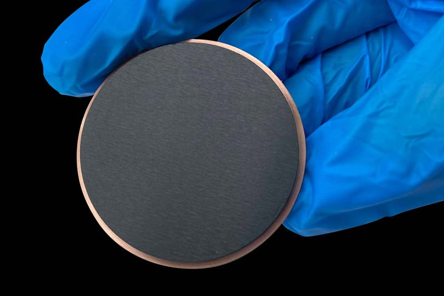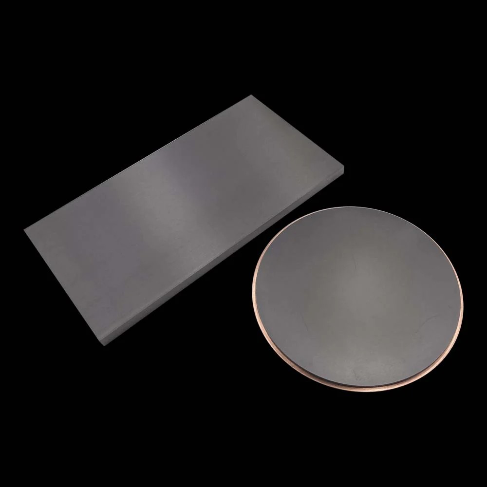
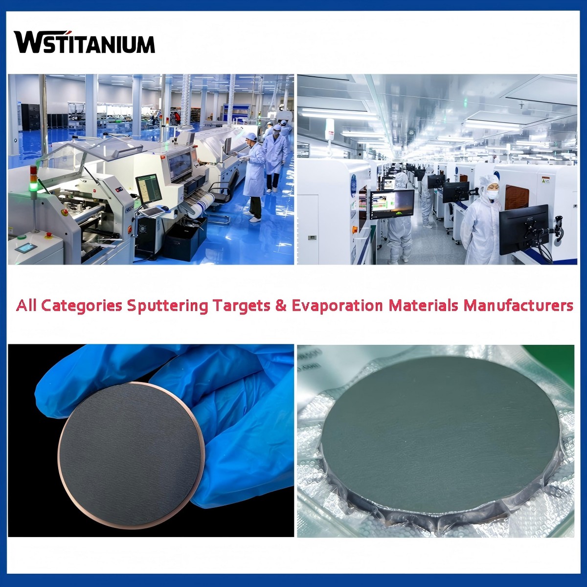
Customized Tantalum(Ta)Sputtering Target
Certified: ISO 9001-2015 & SGS & CE
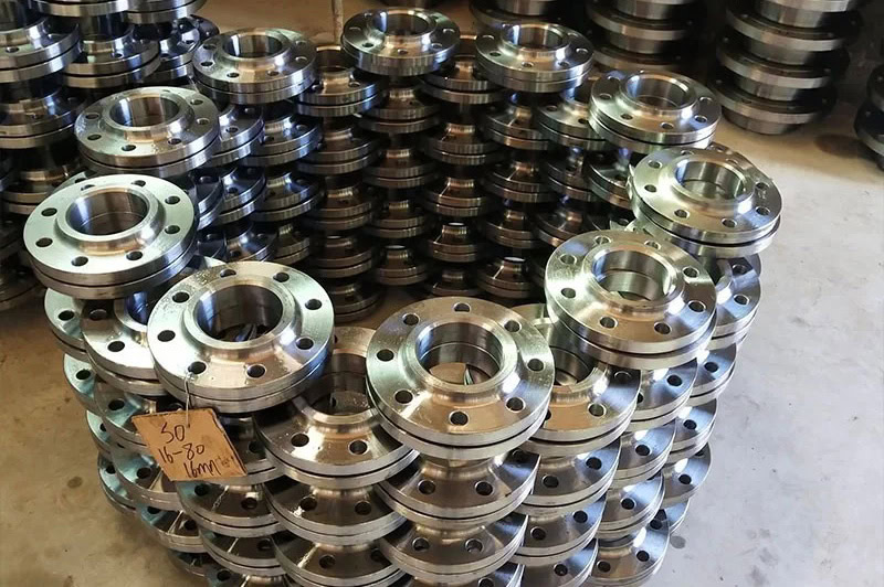
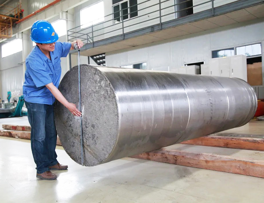
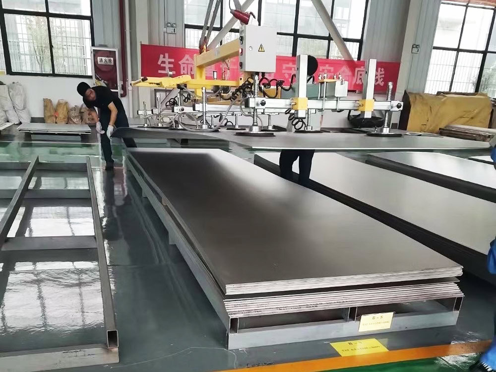
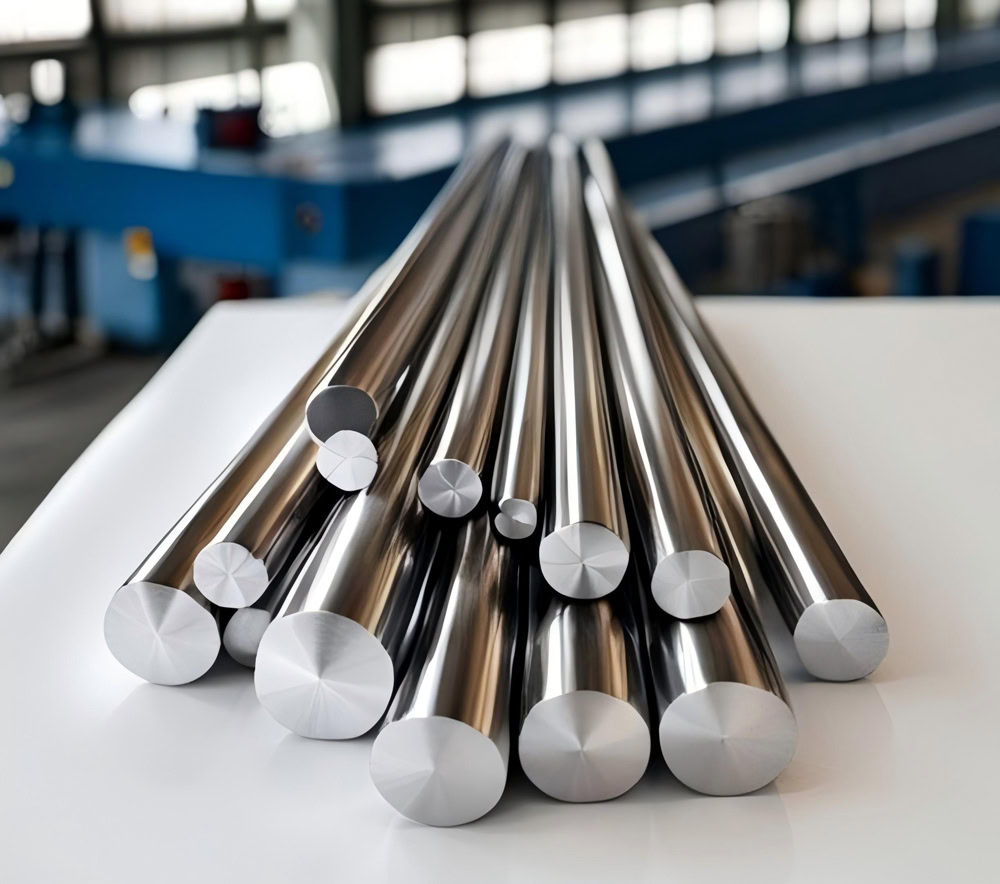
Shape: Requested
Diameter: Customized
Drawings: STEP, IGS , X_T, PDF
Shipping: DHL, Fedex, or UPS & Ocean Freight
Tantalum sputtering target is a key material used in physical vapor deposition (PVD). High-energy ion beams bombard the surface of tantalum sputtering target, causing tantalum atoms to sputter out from the surface of the target and deposit on the substrate material, thus forming a uniform tantalum film. This film has a variety of excellent properties and is widely used in many fields such as semiconductors, electronics, optics, and medical treatment.
Overview
Tantalum (Tantalum), chemical symbol Ta, is a rare metal with unique physical and chemical properties. Its atomic number is 73, and it belongs to the VB group of the sixth period. Tantalum has a low content in the earth’s crust and often coexists with niobium. It mainly exists in ores such as tantalite and niobium-tantalite. Tantalum has a series of excellent properties such as high melting point, low vapor pressure, high chemical stability, strong resistance to liquid metal corrosion, and large dielectric constant of surface oxide film, making it an ideal material for preparing sputtering targets. In nature, tantalum mainly exists in the form of oxides or silicates. Only after complex mineral processing, smelting and purification processes can high-purity metallic tantalum be obtained for the preparation of tantalum sputtering targets.
| Property | Details |
| Density | 16.69 g/cm³ |
| Purity | 99.95% – 99.999% |
| Shape | Customized according to requirements |
| Dimensions | Customizable based on requirements. |
| Symbol | Ta |
| Molar Mass | Approximately 180.95 g/mol |
| Color | Silvery white with metallic luster |
| Atomic Number | 73 |
| Maximum Power Density | Related to equipment and technology |
| Thermal Conductivity | 57.5 W·m⁻¹·K⁻¹ (300K) |
| Melting Point | 3017 °C |
| Thermal Expansion Coefficient | 6.5×10⁻⁶ K⁻¹ (20–100°C) |
| Sputtering Type | DC sputtering, RF sputtering, etc. |
| Electrical Resistivity | 13.5 μΩ·cm |
| Electronegativity | 1.5 (Pauling scale) |
| Heat of Fusion | 36.57 kJ·mol⁻¹ |
| Enthalpy of Vaporization | Approximately 743 kJ·mol⁻¹ |
| Crystal Phase | Body-centered cubic (BCC) lattice |
| Alloys with Other Metals | Ta-Nb, Ta-W, Ta-Mo, Ta-Ti, Ta-Zr, Ta-Ni, Ta-Fe, Ta-Co |
| Compounds with Other Elements | Ta₂O₅, TaC, TaN, TaB₂, TaSi₂, TaP, TaAs, TaSe₂, TaTe₂, LiTaO₃ |
Typical Deposition Conditions
(I) Vacuum degree
In the deposition of tantalum sputtering targets, vacuum degree is a key parameter. Usually, the vacuum degree of the vacuum chamber needs to be pumped to 10⁻⁴ Pa – 10⁻⁷ Pa. In a high vacuum environment, the scattering and collision of gas molecules on the sputtered tantalum atoms are reduced, so that the tantalum atoms reach the substrate surface more directly, thereby improving the deposition rate and quality of the film.
(II) Sputtering power
The size of the sputtering power directly affects the sputtering rate of the target and the quality of the film. Generally speaking, for tantalum sputtering targets, the DC sputtering power density can be controlled at 5 W/cm² – 20 W/cm², and the RF sputtering power density is 10 W/cm² – 50 W/cm². Under lower sputtering power, the target sputtering rate is slower, but a denser film with better crystal quality is obtained; while higher sputtering power can increase the deposition rate, but it may cause problems such as increased internal stress and increased surface roughness of the film. Therefore, it is necessary to reasonably select the sputtering power according to the specific application requirements and film quality requirements.
(III) Gas flow rate
During sputtering, a certain amount of sputtering gas, such as argon (Ar), is usually introduced. The size of the argon flow rate affects the formation and sputtering of plasma. Generally, the argon flow rate can be controlled at 10 sccm – 100 sccm (standard cubic centimeters per minute). An appropriate argon flow rate can ensure the stable generation of plasma, so that the atoms on the target surface can be effectively sputtered out. If the argon flow rate is too small, the plasma density is low and the sputtering efficiency will decrease; if the argon flow rate is too large, it may cause plasma instability and affect the uniformity of the film.
(IV) Substrate temperature
The substrate temperature also has an important influence on the growth and performance of the film. When depositing tantalum film, the substrate temperature can be adjusted between room temperature and 500°C. At a lower substrate temperature, the deposited film usually has higher internal stress and poor crystal quality; while appropriately increasing the substrate temperature can promote the diffusion and migration of film atoms, improve the crystal quality of the film, reduce internal stress, and may also affect the crystal orientation and surface morphology of the film. For example, in some applications, by precisely controlling the substrate temperature, tantalum films can be preferentially grown on specific crystal planes to obtain the required electrical and mechanical properties.
Physical vapor deposition (PVD)
Sputtering deposition: This is one of the most commonly used tantalum film deposition methods. It uses a high-energy ion beam (such as argon ions) generated by an ion source to bombard the surface of the tantalum sputtering target. Under the impact of the ions, the tantalum atoms on the surface of the target obtain enough energy to sputter out from the surface of the target, and fly to the surface of the substrate in a vacuum environment, gradually depositing to form a thin film. Sputtering deposition has the advantages of high deposition rate, strong bonding between the film and the substrate, and precise control of the film composition and thickness. It is suitable for the preparation of high-quality tantalum films and is widely used in semiconductors, optics and other fields.
Evaporation deposition: The tantalum target is evaporated by heating. The evaporated tantalum atoms fly freely in a vacuum and then deposit on the surface of the substrate to form a thin film. The advantages of evaporation deposition are that the equipment is relatively simple and the purity of the film is high, but the deposition rate is relatively low, and the uniformity and adhesion of the film may not be as good as sputtering deposition. In some special applications where the purity of the film is extremely high, but the deposition rate and uniformity are relatively low, such as some high-end optical coating fields, evaporation deposition still has certain applications.
Chemical vapor deposition (CVD)
Chemical vapor deposition is the process of using gaseous tantalum compounds (such as tantalum pentachloride TaCl₅, etc.) to react chemically under high temperature and catalyst to decompose tantalum atoms and deposit them on the surface of the substrate to form a thin film. CVD achieves uniform thin film deposition on substrates of complex shapes and precisely controls the chemical composition and crystal structure of the film. However, CVD equipment is relatively complex, strictly controls parameters such as the flow rate, temperature and pressure of the reaction gas, and is relatively expensive. In semiconductor manufacturing, for some high aspect ratio structures, such as high and deep channels in 3D NAND flash memory, CVD technology is often used to deposit tantalum films as barrier layers and conductive layers to meet their special structural and performance requirements.
Advantages of Tantalum Film
High conductivity: Tantalum film has good conductivity and low resistivity, and can be used as a conductive material in electronic devices. For example, in integrated circuits, tantalum film is often used to make interconnects and electrodes, effectively transmitting current and ensuring the normal operation of electronic devices. Low resistivity reduces the energy loss of electrons when transmitting in tantalum film, improving the operating efficiency and speed of the device.
High reflectivity: Tantalum film has a high reflectivity for light of a specific wavelength and can be used to manufacture optical components such as optical reflectors and laser lenses. In some high-end optical instruments, such as the reflectors of astronomical telescopes, tantalum film is used as a reflective coating to effectively improve the reflection efficiency of light and enhance the observation ability of the instrument.
Adjustable optical properties: By controlling the thickness, microstructure and deposition technology of tantalum film, its optical properties can be precisely adjusted to meet the needs of different optical applications.
High hardness and wear resistance: Tantalum film has high hardness and good wear resistance, and can resist external mechanical wear and scratches to a certain extent. This makes tantalum film perform well in some applications that require long-term use and have high requirements for surface integrity, such as surface coating of cutting tools and molds. After tantalum film coating treatment, the service life of cutting tools and molds is significantly extended, and cutting performance and machining accuracy are also improved.
Good adhesion: Under appropriate deposition conditions, tantalum film has good adhesion to the substrate material, can be firmly combined and not easy to fall off. This feature ensures the stability and reliability of tantalum film in various applications.
Excellent corrosion resistance: Tantalum has extremely high chemical stability, and tantalum film shows excellent corrosion resistance in corrosive environments such as acids and alkalis. This makes tantalum film widely used in chemical, marine and other fields, for example, in chemical reactors.
Biocompatibility: Tantalum film has good biocompatibility and will not produce obvious toxicity and immune response to organisms. Therefore, it has important applications in the medical field, such as surface coating for the manufacture of artificial joints, bone nails and other implantable medical devices, which can reduce the body’s rejection of implants, promote tissue growth and healing, and improve the safety and effectiveness of medical devices.
Applications
(I) Semiconductor industry
In ultra-large-scale integrated circuits, with the continuous reduction of chip size and the continuous improvement of integration, copper interconnection technology has gradually replaced aluminum interconnection technology. However, the diffusion of copper atoms in silicon-based materials will lead to device performance degradation or even failure. Tantalum film effectively prevents copper atoms from diffusing into surrounding materials such as silicon and silicon dioxide, ensuring the stability and reliability of the device, and is one of the key materials for realizing high-performance integrated circuits.
Electrode material: Tantalum film is used as an electrode material in storage devices such as dynamic random access memory (DRAM) and 3D NAND flash memory. Its good conductivity and chemical stability ensure that the electrode can stably transfer charge during the reading and writing process of the storage device, realizing fast storage and reading of data.
(II) Electronic industry
Capacitor: Tantalum capacitor is a high-performance capacitor with the advantages of high capacitance, low leakage current, low equivalent series resistance, good high and low temperature characteristics, and long service life. It is widely used in various electronic devices. Tantalum sputtering target is used to prepare the anodized film of tantalum capacitors, and the performance of the capacitor is optimized by precisely controlling the thickness and quality of the film. In portable electronic devices such as mobile phones, computers, and tablet computers, the demand for miniaturization and high performance of tantalum capacitors continues to drive the development of tantalum sputtering target technology.
Sensors: In some sensors, such as pressure sensors and temperature sensors, tantalum films are used as sensitive materials or electrode materials. Its excellent physical properties and chemical stability enable the sensor to accurately sense the changes in physical quantities under different environmental conditions and convert them into electrical signal outputs. For example, in a pressure sensor, the resistance value of the tantalum film changes with the change in pressure. By measuring the change in resistance value, the pressure can be accurately measured. It is widely used in automobiles, aerospace, industrial automation and other fields.
(III) Optical industry
High reflectivity coating: Because tantalum film has high reflectivity for light of a specific wavelength, it is widely used to manufacture high reflectivity coatings for optical components such as optical reflectors and laser lenses. In laser systems, high-reflectivity tantalum film coatings can improve the reflection efficiency of lasers, reduce the loss of laser energy, and enhance the output power and stability of lasers. In high-end optical instruments, such as astronomical telescopes and microscopes, reflectors coated with tantalum film can provide clearer and brighter images and improve the observation accuracy and resolution of instruments.
Optical filter: By precisely controlling the thickness and microstructure of tantalum film, thin films with specific optical filtering characteristics can be prepared. These optical filters can selectively transmit or absorb light of different wavelengths and are widely used in optical communications, spectral analysis, biomedical imaging and other fields. In optical communication systems, optical filters are used to separate and combine optical signals of different wavelengths, realize the multiplexing and demultiplexing of optical signals, and improve the transmission capacity and efficiency of optical communication systems.
(IV) Medical industry
Implantable medical devices: The biocompatibility of tantalum makes tantalum film an important application in the field of implantable medical devices. For example, coating tantalum film on the surface of medical devices such as artificial joints, bone screws, and heart stents can reduce the body’s rejection of implants and promote tissue growth and healing.
Medical equipment parts: Some medical equipment parts, such as the anode target of X-ray tubes and the electron emission source of electron microscopes, also use tantalum or tantalum alloy materials. Tantalum’s high melting point, good conductivity and thermal stability enable these parts to operate stably under high-energy and high-temperature working conditions, ensuring the normal operation and accurate diagnosis of medical equipment.
Conclusion
Tantalum sputtering targets, as a key material, have a wide range of important applications in semiconductors, electronics, optics, medical treatment, aerospace and many other fields due to their unique physical and chemical properties and excellent film properties.